


98 www.xilinx.com PowerPC™ 405 Processor Block Reference Guide
1-800-255-7778 UG018 (v2.0) August 20, 2004
Chapter 2: Input/Output Interfaces
R
Device-Control Register Interfaces
The device-control register (DCR) interface provides a mechanism for the processor block
to initialize and control peripheral devices that reside on the same FPGA chip. For
example, the memory-transfer characteristics and address assignments for a bus-interface
unit (BIU) can be configured by software using DCRs. The DCRs are accessed using the
PowerPC mfdcr and mtdcr instructions. The addressing used by these instructions is not
memory mapped and thus does not interfere with OCM/PLB memory addressing. All
device control registers are defined in a 10-bit, word-aligned range.
The following types of device-control register (DCR) interfaces exist:
x PowerPC block internal device-control register interface.
x General purpose DCR bus interface.
x Dedicated EMAC DCR bus interface (Virtex-4-FX only).
The subsequent sections will describe these interfaces and highlight differences between
the Virtex-II Pro/ProX and Virtex-4-FX DCR functionary
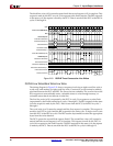
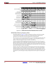
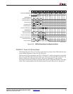
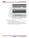
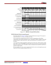
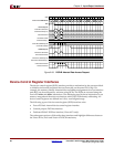
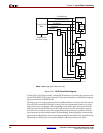
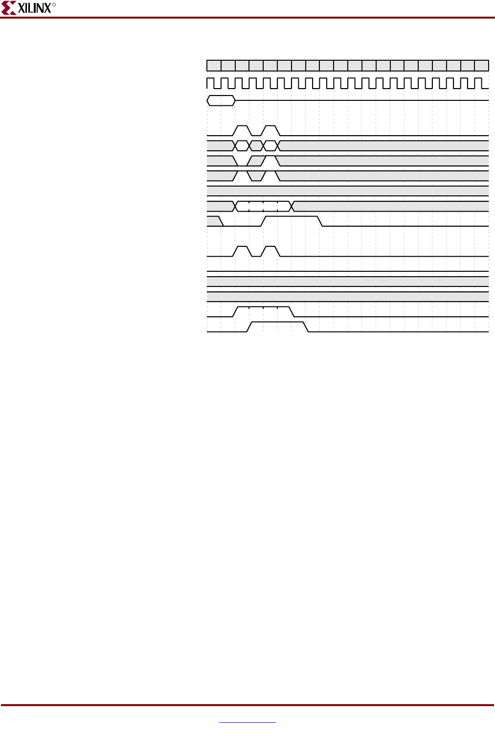
Figure 2-28: DSPLB Aborted Data-Access Request
Cy cle
1 2 3 4 5 6 7 8 9 10 11 12 13 14 15 16 17 18 19 20
PLBCLK and CPMC405CLK
UG018_32_101701
PPC405 Outputs:
C405PLBDCUREQUEST
C405PLBDCURNW
C405PLBDCUABUS[0:31]
adr1 adr2
flush1
C405PLBDCUBE[0:7]
C405PLBDCUWRDBUS[0:63]
C405PLBDCUSIZE2
C405PLBDCUABORT
PLB/BIU Outputs:
PLBC405DCUADDRACK
PLBC405DCURDDBUS[0:63]
PLBC405DCURDWDADDR[1:3]
PLBC405DCURDDACK
PLBC405DCUWRDACK
PLBC405DCUBUSY
DCU
rl2wl1
rl2wl1
wl1
01
wl1
23
wl1
45
wl1
67
d1
01
d1
23
d1
45
d1
67