


PowerPC™ 405 Processor Block Reference Guide www.xilinx.com 107
UG018 (v2.0) August 20, 2004 1-800-255-7778
R
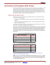
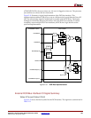
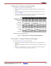
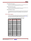
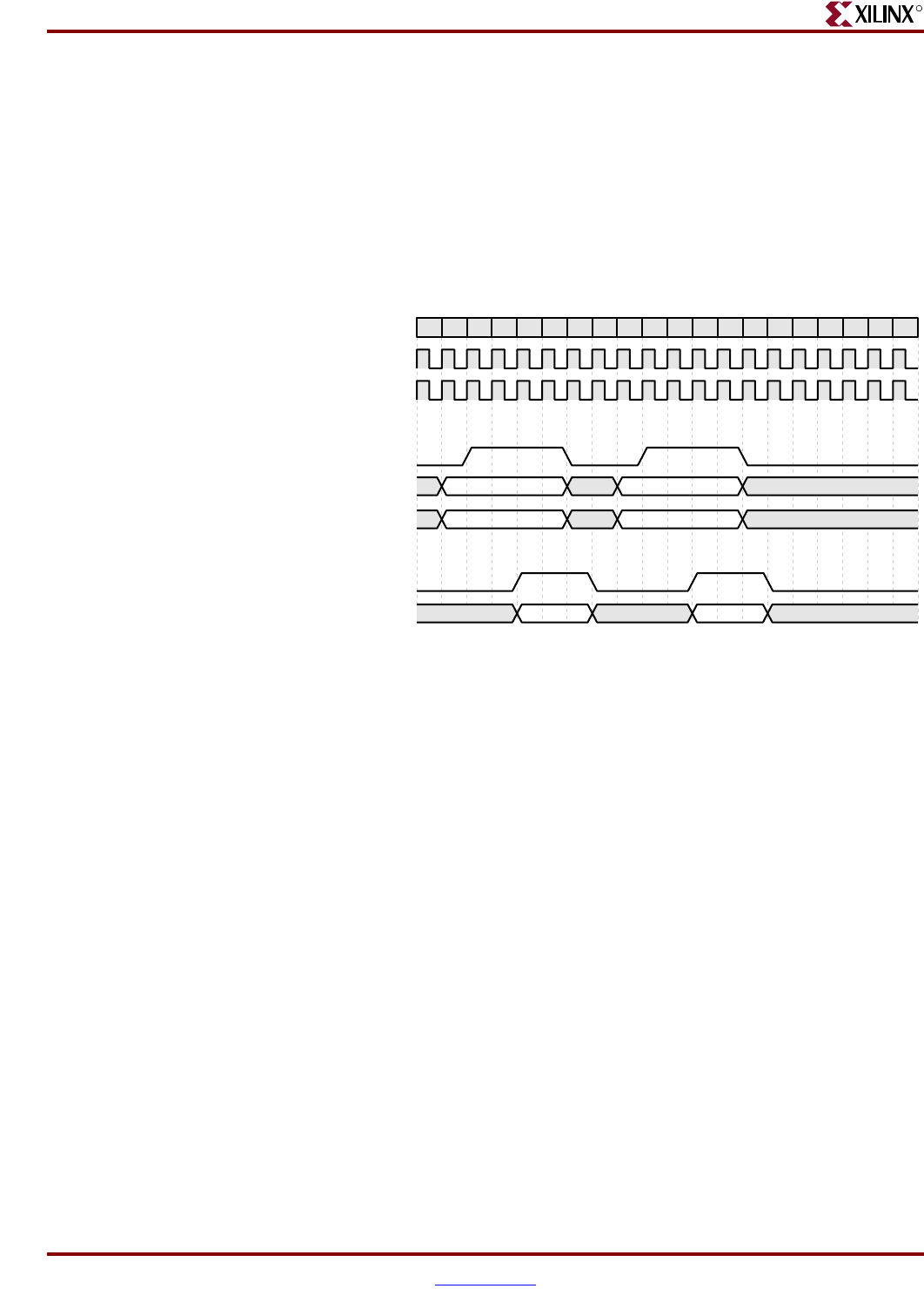
DCR Interface 1:1 Clocking, Latched Acknowledge
The example in Figure 2-33 assumes the following:
x The PowerPC 405 and the peripheral containing the DCR are clocked at the same
frequency.
x The acknowledge signal is latched and forwarded with the DCR bus as shown in
Figure 2-31, page 103.
x After the acknowledge signal is asserted, it is not deasserted until the appropriate
read-access or write-access request signal is deasserted.
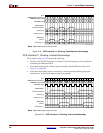
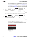
DCR Interface 1:1 Clocking, Combinatorial Acknowledge
The example in Figure 2-34 assumes the following:
x The PowerPC 405 and the peripheral containing the DCR are clocked at the same
frequency.
x The acknowledge signal is generated by combinatorial logic from the DCR read/write
signal.
x After the acknowledge signal is asserted, it is not deasserted until the appropriate
read-access or write-access request signal is deasserted.
Figure 2-33: DCR Interface 1:1 Clocking, Latched Acknowledge
Cy cle
CPMC405CLOCK (Virtex-II Pro)/
CPMDCRCLK (Virtex-4 FX)
1 2 3 4 5 6 7 8 9 10 11 12 13 14 15 16 17 18 19 20
DCR (FPGA) Clock
UG018_41_032504
DCRWRITE/DCRREAD
DCRABUS[0:9]
PPC405 Outputs:
DCRDBUSOUT[0:31]
DCRDBUSIN[0:31]
DCRACK
DCR Outputs:
data0 data1
addr0 addr1
data0 data1
Note: Abbreviated signal names are used.