


92 www.xilinx.com PowerPC™ 405 Processor Block Reference Guide
1-800-255-7778 UG018 (v2.0) August 20, 2004
Chapter 2: Input/Output Interfaces
R
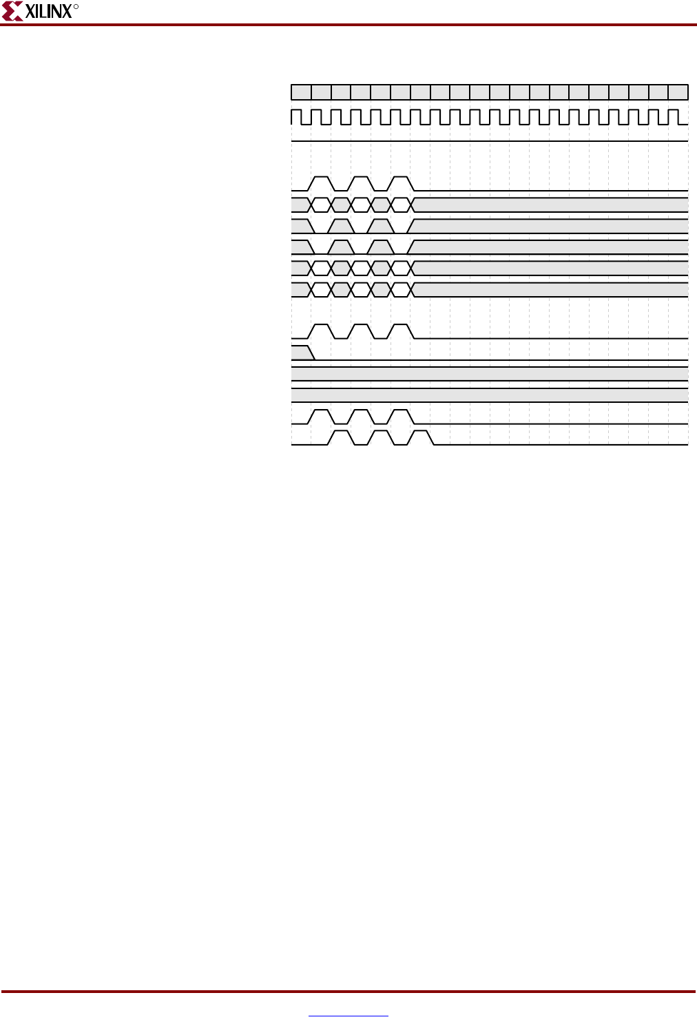
DSPLB Line Write/Line Read/Word Write
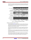
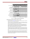
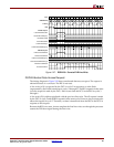
The timing diagram in Figure 2-23 shows a sequence involving an eight-word line write,
an eight-word line read, and a word write. It provides an example of address pipelining
involving writes and reads. It also demonstrates how read and write operations can
overlap due to the split read-data and write-data busses.
The first line write (wl1) is requested by the DCU in cycle 3 in response to a cache flush
(represented by the flush1 transaction in cycles 1 through 2). The BIU responds in the same
cycle the request is made by the DCU. Data is sent from the DCU to the BIU in cycles 3
through 6.
The first line read (rl2) is address pipelined with the previous line write. The rl2 request is
made by the DCU in cycle 5 and the BIU responds in the same cycle. Data is sent from the
BIU to the DCU fill buffer in cycles 6 through 9. Because of the split data bus, a read
operation overlaps with a previous write operation in cycle 6. After all data associated
with this line is read, it is transferred by the DCU from the fill buffer to the data cache. This
is represented by the fill2 transaction in cycles 10 through 12.
The word write (ww3) cannot be requested until the first write request (wl1) is complete
because address pipelining of multiple write requests is not supported. However, this
request is address pipelined with the previous line read request (rl2). The ww3 request is
made by the DCU in cycle 8 and the BIU responds in the same cycle. A single word is sent
from the DCU to the BIU in cycle 8. The BIU uses the byte enables to select the appropriate
bytes from the write-data bus. Because of the split data bus, this write operation overlaps
with a read operation from the previous read request (rl2).
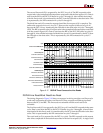
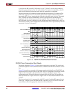
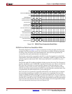
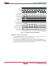
Figure 2-22: DSPLB Three Consecutive Word Writes
Cy cle
1 2 3 4 5 6 7 8 9 10 11 12 13 14 15 16 17 18 19 20
PLBCLK and CPMC405CLK
UG018_26_101701
PPC405 Outputs:
C405PLBDCUREQUEST
C405PLBDCURNW
C405PLBDCUABUS[0:31]
adr1 adr2 adr3
val val val
d1 d2 d3
C405PLBDCUBE[0:7]
C405PLBDCUWRDBUS[0:63]
C405PLBDCUSIZE2
DCU
ww2 ww3ww1
PLB/BIU Outputs:
PLBC405DCUADDRACK
PLBC405DCURDDBUS[0:63]
PLBC405DCURDWDADDR[1:3]
PLBC405DCURDDACK
PLBC405DCUWRDACK
PLBC405DCUBUSY
ww2 ww3ww1
ww2 ww3ww1