


106 www.xilinx.com PowerPC™ 405 Processor Block Reference Guide
1-800-255-7778 UG018 (v2.0) August 20, 2004
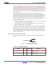
Chapter 2: Input/Output Interfaces
R
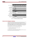
The processor does not begin driving a new DCR address until the DCR acknowledge
signal corresponding to the previous DCR access has been deasserted for at least one cycle.
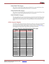
C405DCRDBUSOUT[0:31]/EXTDCRDBUSOUT[0:31] (Output)
This write-data bus is driven by the processor block when a mtdcr or mfdcr instruction is
executed. Its contents are valid only when a DCR write-request or DCR read-request is
asserted. When a mtdcr instruction is executed, this bus contains the data to be written into
a DCR. When a mfdcr instruction is executed, this bus contains the value 0x0000_0000.
During reset, this bus is driven with the value 0x0000_0000. Peripherals can use this value
to initialize the DCRs.
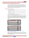
DCRC405ACK/EXTDCRACK (Input)
When asserted, this signal indicates a peripheral device acknowledges the processor block
request for DCR access. A peripheral device should assert this signal only when all of the
following are true:
x The peripheral device contains the addressed DCR.
x A DCR read or write request exists.
x The peripheral device is driving the DCR data bus (read access).
x The peripheral device latched the DCR data bus (write access).
The acknowledgement should not be deasserted until the read/write signal is deasserted.
This allows the PowerPC 405 and peripheral device to be clocked at different frequencies
without affecting the interface handshaking protocol.
The processor block waits up to 64 processor core clock (CPMC405CLOCK) cycles for a
read/write request to be acknowledged. If a DCR does not acknowledge the request in this
time, the access times out. No error occurs when a DCR access is timed-out, the processor
simply goes on to execute the next instruction.
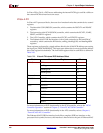
DCRC405DBUSIN[0:31]/EXTDCRDBUSIN[0:31] (Input)
This read-data bus is latched by the processor block when a peripheral device asserts the
DCR acknowledge signal in response to a DCR read-access request. A peripheral device
must drive this bus only when it contains the accessed DCR and the DCR read-access
signal is asserted by the processor block.
Peripheral devices should drive only the bits implemented by the specified DCR. A value
of 0x0000_0000 is driven onto the DCR write-data bus by the processor block during a
read-access request. This value is passed along the DCR chain until modified by the
appropriate peripheral. The end of the DCR chain is attached to the DCR read-data bus
input to the processor block. Thus, the processor reads the updated value of all
implemented bits, and unimplemented (and unattached) bits retain a value of 0.
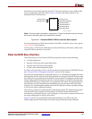
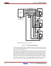
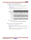
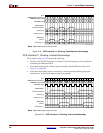
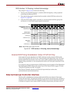
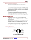
External DCR Bus Interface Timing Diagrams
The following timing diagrams show typical transfers that can occur on the DCR interface
using the two interface modes. Unless otherwise noted, optimal timing relationships are
used to improve the readability of the timing diagrams. The assertion of
DCRREAD/DCRWRITE refers to a read or
write operation, not both. The processor block
cannot perform a simultaneous read and write of the DCR bus.