


136 www.xilinx.com PowerPC™ 405 Processor Block Reference Guide
1-800-255-7778 UG018 (v2.0) August 20, 2004
Chapter 2: Input/Output Interfaces
R
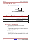
Additional FPGA Specific Signals
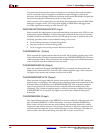
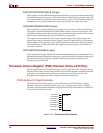
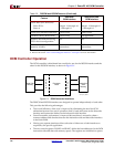
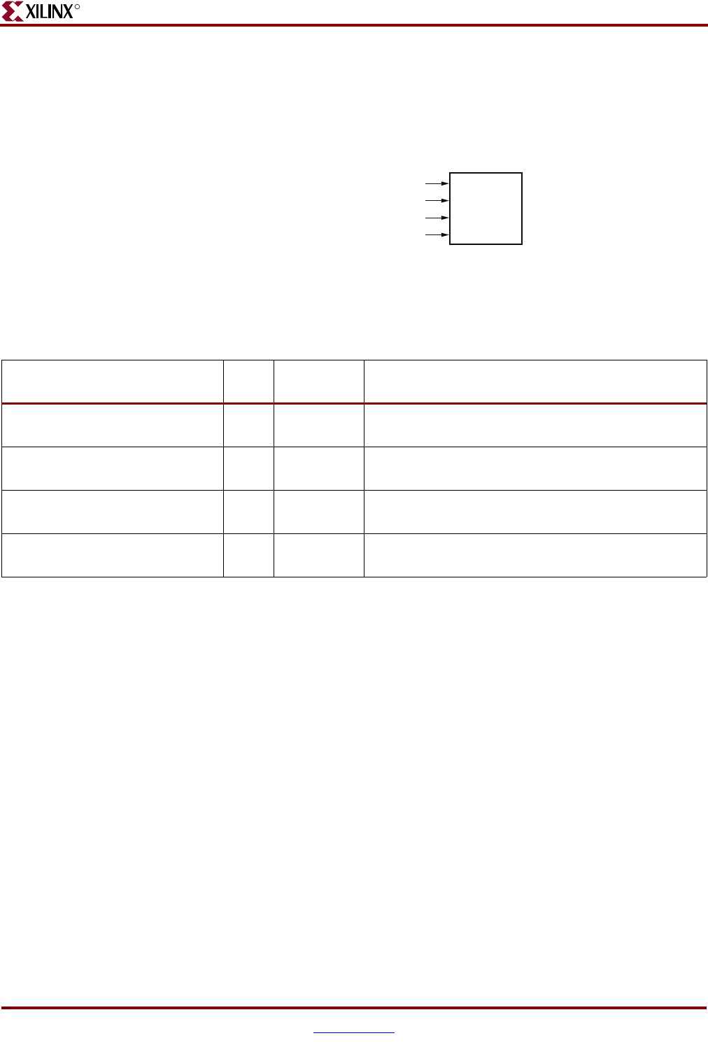
Figure shows the block symbol for the additional FPGA signals used by the processor
block. The signals are summarized in Table 2-30.
Additional FPGA I/O Signal Descriptions
The following sections describe the operation of the FPGA I/O signals.
MCBCPUCLKEN (Input)
When asserted, this signal indicates that the enable for the core clock zone
(CPMC405CPUCLKEN) should follow (match the value of) the global write enable (GWE)
during the FPGA startup sequence. When deasserted, the enable for the core clock zone
ignores (is independent of) the value of GWE.
MCBJTAGEN (Input)
When asserted, this signal indicates that the enable for the JTAG clock zone
(CPMC405JTAGCLKEN) should follow (match the value of) the global write enable (GWE)
during the FPGA startup sequence. When deasserted, the enable for the JTAG clock zone
ignores (is independent of) the value of GWE.
Figure 2-49: FPGA Specific Interface Block Symbol
PPC405
MCBCPUCLKEN
MCBJTAGENT
MCBTIMEREN
MCPPCRST
UG018_02_49_032504
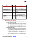
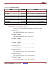
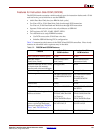
Table 2-30: Additional FPGA I/O Signals
Signal
I/O
Type
If Unused Function
MCBCPUCLKEN I 1 Indicates the PowerPC 405 clock enable should follow
GWE during a partial reconfiguration.
MCBJTAGEN I 1 Indicates the JTAG clock enable should follow GWE
during a partial reconfiguration.
MCBTIMEREN I 1 Indicates the timer clock enable should follow GWE
during a partial reconfiguration.
MCPPCRST I 1 Indicates the processor block should be reset when
GSR is asserted during a partial reconfiguration.