


66 www.xilinx.com PowerPC™ 405 Processor Block Reference Guide
1-800-255-7778 UG018 (v2.0) August 20, 2004
Chapter 2: Input/Output Interfaces
R
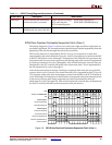
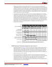
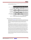
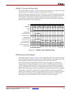
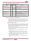
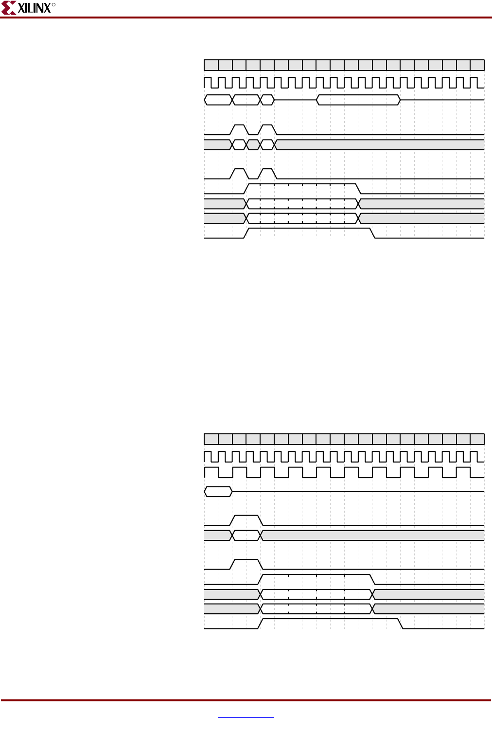
ISPLB 2:1 Core-to-PLB Line Fetch
The timing diagram in Figure 2-12 shows an eight-word line fetch in a system with a PLB
clock that runs at one half the frequency of the PowerPC 405 clock.
The line read (rl1) is requested by the ICU in PLB cycle 2, which corresponds to PowerPC
405 cycle 3. The BIU responds in the same cycle. Instructions are sent from the BIU to the
ICU fill buffer in PLB cycles 3 through 6 (PowerPC 405 cycles 5 through 12). After all
instructions associated with this line are read, the line is transferred by the ICU from the fill
buffer to the instruction cache (not shown).
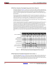
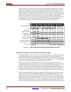
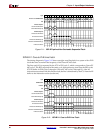
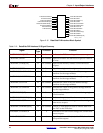
Figure 2-11: ISPLB Pipelined Non-Cacheable Sequential Fetch
Cy cle
1 2 3 4 5 6 7 8 9 10 11 12 13 14 15 16 17 18 19 20
PLBCLK and CPMC405CLK
UG018_16_101701
PPC405 Outputs:
C405PLBICUREQUEST
C405PLBICUABUS[0:29]
adr1 adr2
byp2byp1prefetch2miss1
ICU
rl2rl1
rl2rl1
PLB/BIU Outputs:
PLBC405ICUADDRACK
PLBC405ICURDDBUS[0:63]
PLBC405ICURDWDADDR[1:3]
PLBC405ICURDDACK
rl1
67
rl1
01
rl1
23
rl1
45
rl2
01
rl2
23
rl2
45
rl2
67
d1
67
d1
01
d1
23
d1
45
d2
01
d2
23
d2
45
d2
67
02466024
PLBC405ICUBUSY
Figure 2-12: ISPLB 2:1 Core-to-PLB Line Fetch
Cy cle
1 2 3 4 5 6 7 8 9 10 11 12 13 14 15 16 17 18 19 20
CPMC405CLK
UG018_18_101701
PPC405 Outputs:
C405PLBICUREQUEST
C405PLBICUABUS[0:29]
adr1
rl1
rl1
PLB/BIU Outputs:
PLBC405ICUADDRACK
PLBC405ICURDDBUS[0:63]
PLBC405ICURDWDADDR[1:3]
PLBC405ICURDDACK
rl1
01
rl1
23
rl1
45
rl1
67
d1
01
d1
23
d1
45
d1
67
0246
miss1
ICU
PLBCLK
PLBC405ICUBUSY