


36 www.xilinx.com PowerPC™ 405 Processor Block Reference Guide
1-800-255-7778 UG018 (v2.0) August 20, 2004
Chapter 2: Input/Output Interfaces
R
i The DBGC405DEBUGHALT chip-input signal (if provided) is asserted. Assertion
of this signal indicates that an external debug tool wants to control the PowerPC
405 processor. See “DBGC405DEBUGHALT (Input)” for more information.
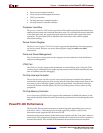
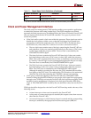
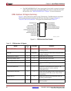
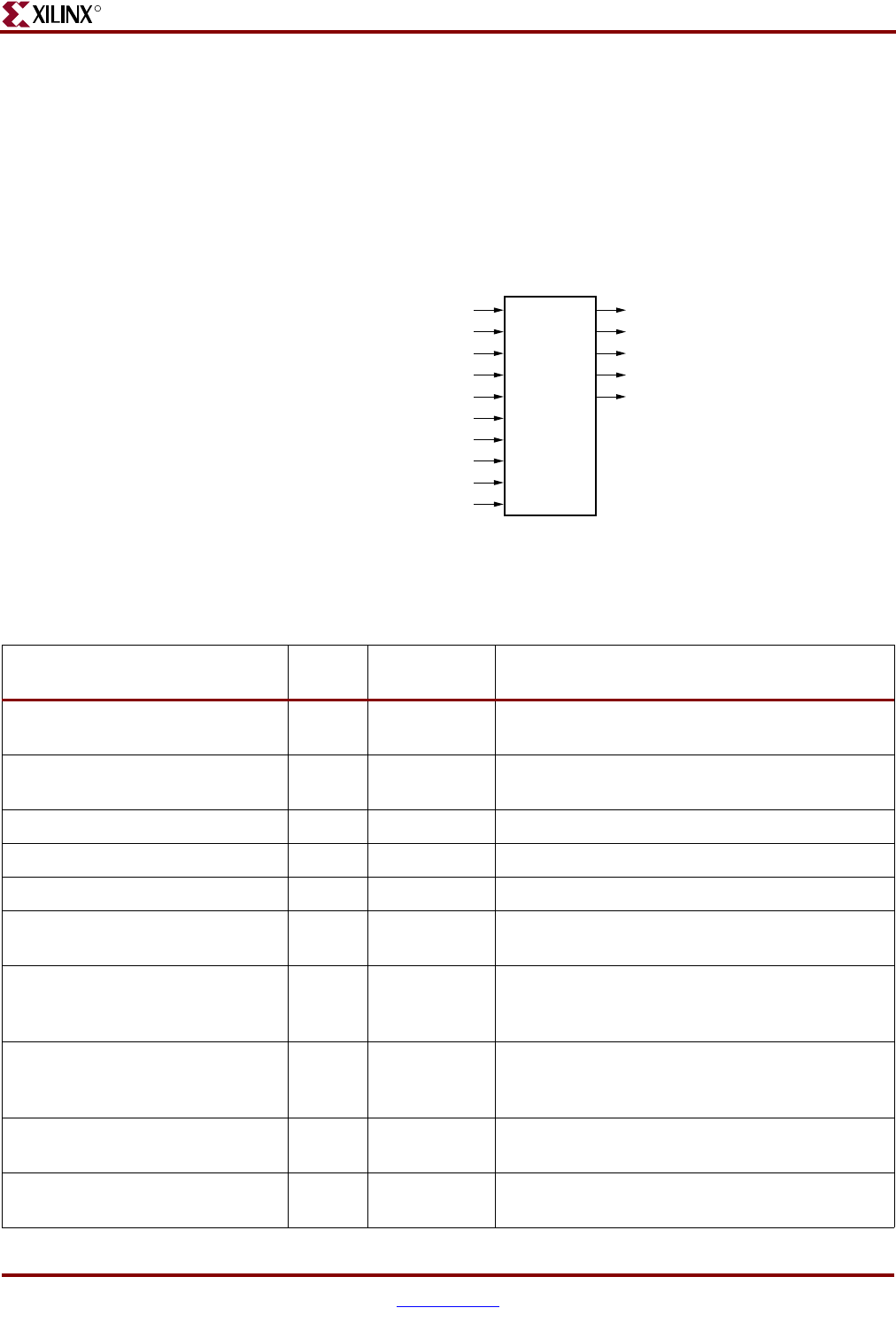
CPM Interface I/O Signal Summary
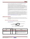
Figure 2-1 shows the block symbol for the CPM interface. The BRAM clocks associated
with the data-side and instruction-side OCM are described in chapter Chapter 3,
“PowerPC 405 OCM Controller.” The signals are summarized in Table 2-2.
Figure 2-1: CPM Interface Block Symbol
PPC405
CPMC405CLOCK
PLBCLK
CPMC405CPUCLKEN
CPMC405TIMERCLKEN
CPMC405JTAGCLKEN
C405CPMMSREE
C405CPMMSRCE
C405CPMTIMERIRQ
C405CPMTIMERRESETREQ
C405CPMCORESLEEPREQ
CPMC405CORECLKINACTIVE
CPMC405TIMERTICK
CPMC405SYNCBYPASS
CPMDCRCLK
CPMFCMCLK
UG018_02_01_051204
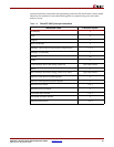
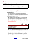
Table 2-2: CPM Interface I/O Signals
Signal
I/O
Type
If Unused Function
CPMC405CLOCK I Required PowerPC 405 clock input (for all non-JTAG logic,
including timers).
PLBCLK I Required PLB clock interface clock (lacks CPM prefix due
to legacy naming).
CPMC405CPUCLKEN I 1 Enables the core clock zone.
CPMC405TIMERCLKEN I 1 Enables the timer clock zone.
CPMC405JTAGCLKEN I 1 Enables the JTAG clock zone.
CPMC405CORECLKINACTIVE I 0 Indicates the CPM logic disabled the clocks to the
core.
CPMC405TIMERTICK I 1 Increments or decrements the PowerPC 405
timers every time it is active with the
CPMC405CLOCK.
CPMC405SYNCBYPASS I 1 Virtex-4-FX only. Bypass PLB re-synchronization
inside the PowerPC 405 core for Virtex-II Pro
compatibility.
CPMDCRCLK I 0 Virtex-4-FX only. DCR bus interface clock for
PPC405 synchronization.
CPMFCMCLK I 0 Virtex-4-FX only. FCM interface clock for the
APU Controller.