


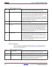

PowerPC™ 405 Processor Block Reference Guide www.xilinx.com 163
UG018 (v2.0) August 20, 2004 1-800-255-7778
R
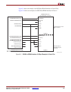
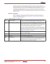
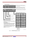
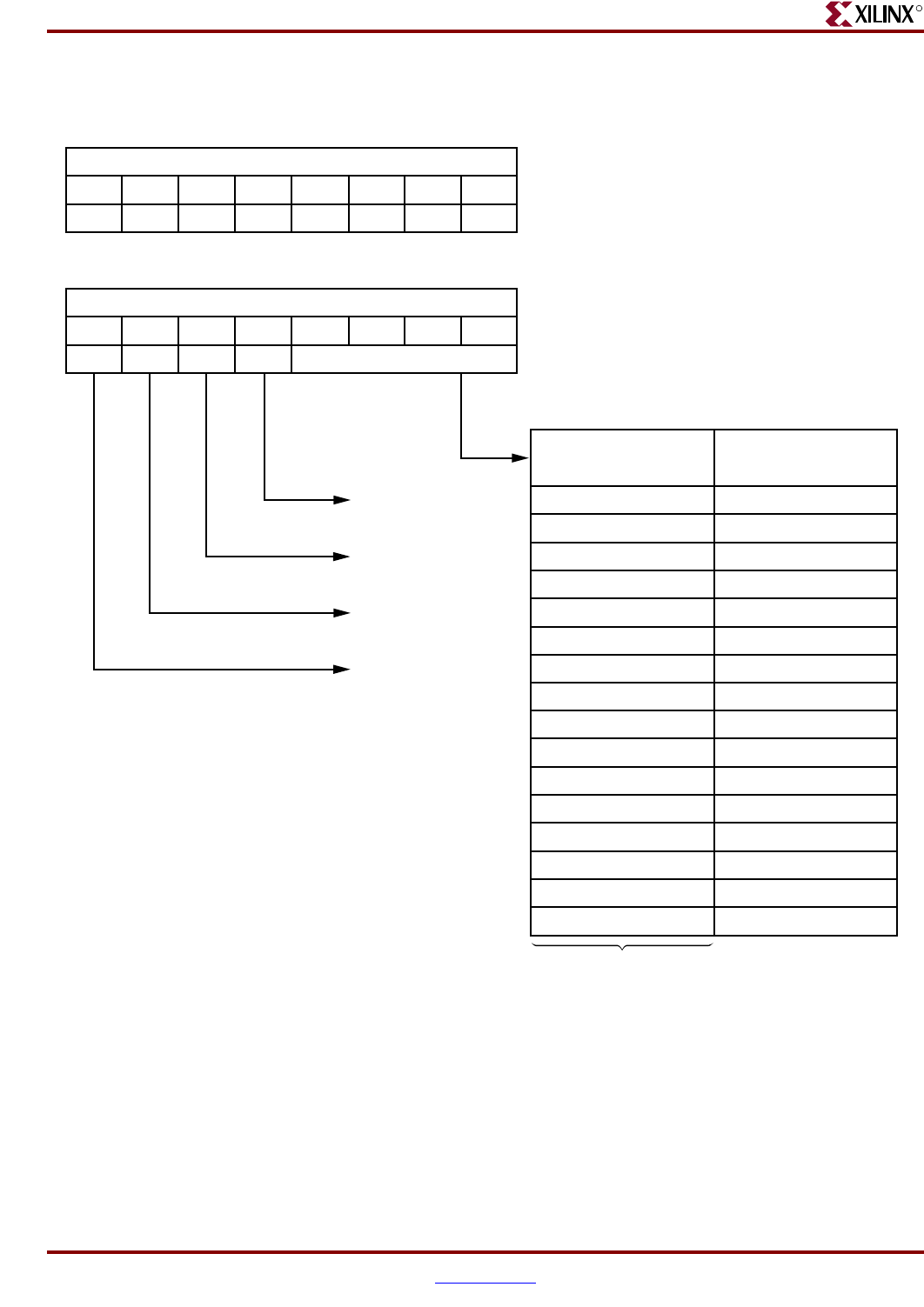
Figure 3-12: DSOCM DCR Registers for Virtex-4
UG018_46b_042304
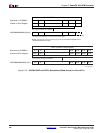
DSARC (DSOCM Address Range Compare Register)
User Programmable Registers
Allocated within DCR address space (Programmer's Model)
8 bits: Address range compare for DSOCM memory space.
They are also configurable via FPGA, through the DSARCVALUE
inputs to the processor block.
Note: The top 8 bits of the CPU address are compared with
DSARC to provide a 16 MB logical address space for DSOCM
block. OCM must be placed in a non-cacheable memory region.
Notes:
1. Recommend 1 for auto clock ratio detection. Additionally, when DSOCMMCM
is read back, the value of the auto-detected clock ratio is reflected in terms
of the wait state value.
2. See section "DSOCM Ports" in the text.
3. DISABLEOPERANDFWD:
When DISABLEOPERANDFWD is asserted, load data from the DSOCM
goes directly into a latch in the processor block. This causes an additional
cycle (a total of two cycles) of latency between a load instruction which
is followed by an instruction that requires the load data as an operand.
When DISABLEOPERANDFWD is not asserted, load data from the DSOCM
must pass through steering logic before arriving at a latch. This causes a
single cycle of latency between a load instruction which is followed by an
instruction that requires the load data as an operand.
4. DSOCMEN:
Enables the DSOCM address decoder.
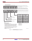
0
A0/P
1
A1/P
5
A5/P
6
A6/P
7
A7/P
2
A2/P
3
A3/P
4
A4/P
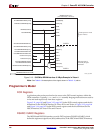
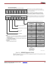
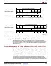
DSCNTL (DCR Control Register)
8 bits: Control Register for DSOCM. They are also configurable v
ia
FPGA, through the DSCNTLVALUE inputs to the processor block.
Legacy support for backward compatibility with Virtex-II Pro
0
D0/P
1
D1/P
5
. . .
[4:7] wait state register
67
D7/P
2
D2/P
3
D3/P
4
D4/P
DSOCMMCM[0:3]
DSOCMEN
(4)
0000
0001
0010
0011
0100
0101
0110
0111
2n - 1
Not supported
1:1
Not supported
2:1
Not supported
3:1
Not supported
4:1
CPMC405CLOCK:
BRAMDSOCMCLK
Ratio
1000
1001
1010
1011
1100
1101
1110
1111
Not supported
5:1
Not supported
6:1
Not supported
7:1
Not supported
8:1
where n = number of
processor clocks in
one BRAM clock cycle.
Must be an integer.
DISABLEOPERANDFWD
(3)
DSOCMBUSY
(2)
Auto clock ratio detection
(1)