


PowerPC™ 405 Processor Block Reference Guide www.xilinx.com 103
UG018 (v2.0) August 20, 2004 1-800-255-7778
R
(CPMC405CLOCK), the access times out. No error is flagged on time-out. The processor
just continues to execute the next instruction.
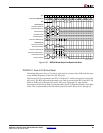
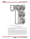
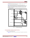
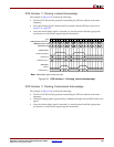
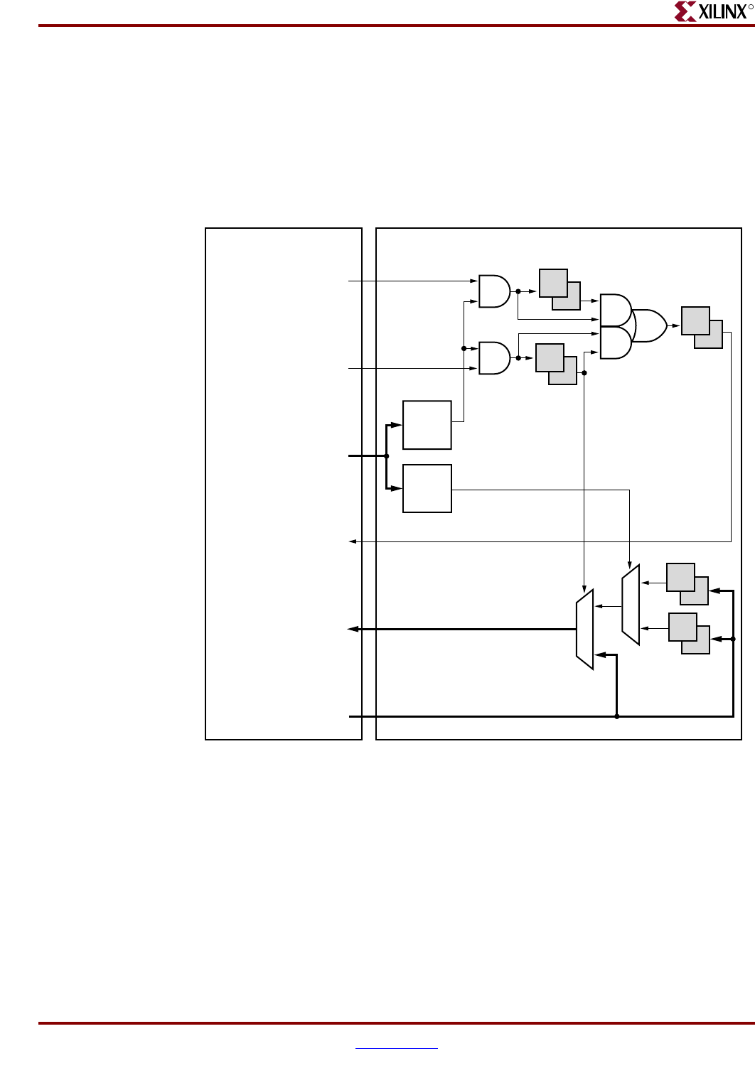
Figure 2-31 illustrates a logical implementation of the DCR bus interface. This
implementation enables a DCR slave to run at a different clock speed than the PowerPC
405. The acknowledge signal is latched and forwarded with the DCR bus. The bypass
multiplexor minimizes data-bus path delays when the DCR is not selected. To ensure
reusability across multiple FPGA environments, all DCR slave logic should use the
specified implementation.
External DCR Bus Interface I/O Signal Summary
Virtex-II Pro and Virtex-II ProX
Figure 2-32 shows the block symbol for the DCR interface. The signals are summarized in
Table 2-21.
Figure 2-31: DCR Bus Implementation
L1
L2
L1
L2
L2
L1
L1
L2
L2
L1
Full
Address
Decode
Lower
Address
Decode
0
1
0
1
DCR2
DCR1
DCR Slave
Processor Core
Bypass Mux
DCRWRITE
DCRREAD
DCRABUS[0:9]
DCRACK
DCRDBUSIN[0:31]
DCRDBUSOUT[0:31]
UG018_53_051204