


208 www.xilinx.com PowerPC™ 405 Processor Block Reference Guide
1-800-255-7778 UG018 (v2.0) August 20, 2004
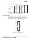
Appendix A: RISCWatch and RISCTrace Interfaces
R
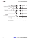
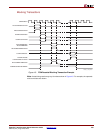
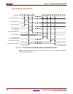
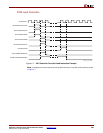
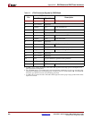
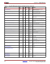
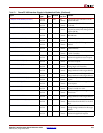
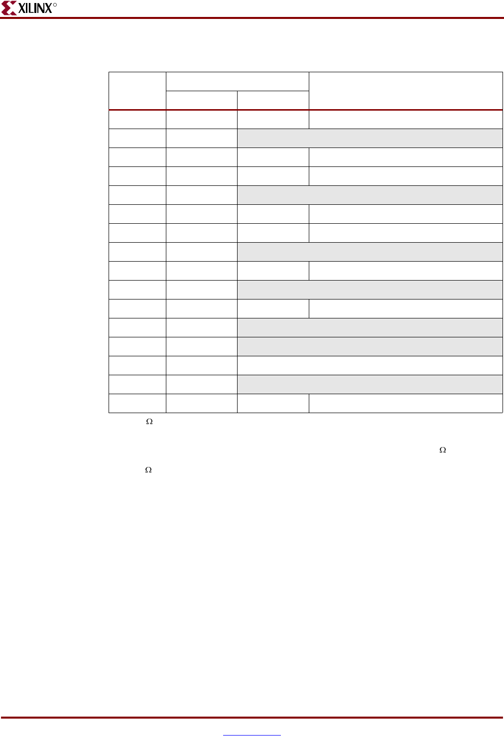
Table A-1: JTAG Connector Signals for RISCWatch
Pin
RISCWatch
Description
I/O Signal Name
1 Input TDO JTAG test-data out.
2 No Connect
Reserved
3OutputTDI
a
a. A 10 K pull-up resistor should be connected to this signal to reduce chip-power consumption. The
pull-up resistor is not required.
JTAG test-data in.
4 Output TRST JTAG test reset.
5 No Connect
Reserved
6Output+Power
b
b. The +POWER signal, is provided by the board, and indicates whether the processor is operating. This
signal does not supply power to the debug tools or to the processor. A series resistor (1 K
or less) should
be used to provide short-circuit current-limiting protection.
Processor power OK
7OutputTCK
c
c. A 10 K pull-up resistor must be connected to these signals to ensure proper chip operation when these
inputs are not used.
JTAG test clock.
8 No Connect
Reserved
9 Output TMS JTAG test-mode select.
10 No Connect
Reserved
11 Output HALT Processor debug halt mode.
12 No Connect
Reserved
13 No Connect Reserved
14 KEY No pin should be placed at this position.
15 No Connect
Reserved
16 GND Ground