


PowerPC™ 405 Processor Block Reference Guide www.xilinx.com 169
UG018 (v2.0) August 20, 2004 1-800-255-7778
R
BRAMs that interface with the ISOCM controller can also be initialized through the
configuration bit-stream, during FPGA configuration. The Data2MEM software utility in
the design flow tools can be used to load ISBRAM and DSBRAM with instructions and
data respectively.
Timing Specification for Fixed Latency (Virtex-4 and Virtex-II Pro)
The single-cycle and multi-cycle operation modes are designed to guarantee a certain
performance level by the OCM controllers, assuming a certain processor frequency and
quantity of BRAMs. As additional BRAMs are added to a design, the processor clock
frequency must be reduced or wait states must be added in the processor block to insure
that the OCM interface operates correctly. When the processor and OCM controller clocks
operate at integer multiples of each other, wait cycles are automatically added inside the
processor block. The processor core and OCM controllers must be aligned on rising edges
of their respective clocks.
The frequency of the OCM to BRAM interface is determined by running the design
through the Xilinx design implementation tools and performing timing analysis on the
interface. The interface timing is dependent upon the BRAM memory organization, signal
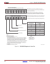
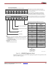
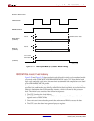
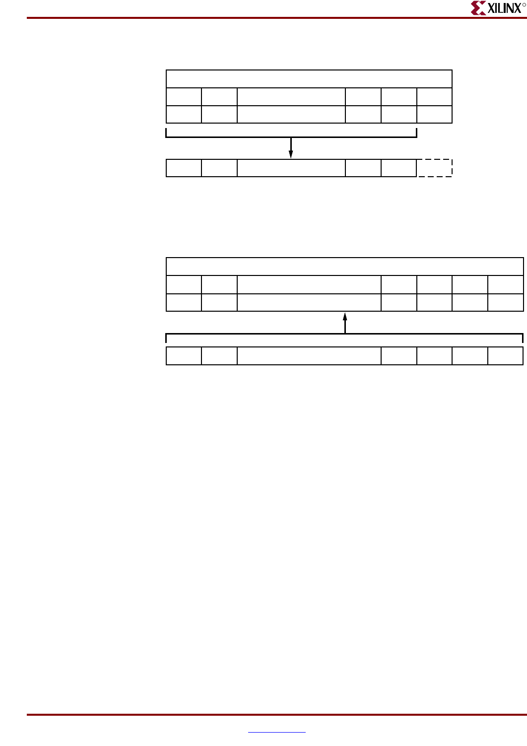
Figure 3-17: ISOCM: ISINIT and ISFILL Descriptions (Read Access), for Virtex-4
UG018_69b_05120
4
R
ead Data on DCRDBUS
C
ontent in ISINIT Register
ISINIT (ISOCM Initialization Address)
. . . .
. . . .
D 8
Bit 8
Map to physical address bus to ISBRAM
Bit 8 to Bit 28 of ISINIT register value maps to 21 bit initialization address for ISOCMBRAMWRABUS [ 8:28 ].
The address represented by A8 to A29 is increased by 1 for every write into the ISFILL register.
Bit 29 of ISINIT register is used to interface to the processor block to generate the ISOCMBRAMEVENWRITEEN/
ISOCMBRAMODDWRITEEN, and ISOCMDCRBRAMEVENEN/ISOCMDCRBRAMODDEN outputs.
D 9
Bit 9
D 27
Bit 27
D 28
Bit 28
D 29
Bit 29
I
SOCMBRAMWRABUS[ 8:28 ]
. . . .
A 8 A 9 A 27 A 28
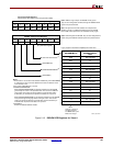
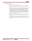
R
ead Data on DCRBUS
C
ontent in ISFILL Register
ISFILL (ISOCM Fill Data Register)
. . . .
. . . .
D 0
Bit 0
Map from physical read data bus to ISBRAM
D 1
Bit 1
D 28
Bit 28
D 29
Bit 29
D 30
Bit 30
D 31
Bit 31
B
RAMISOCMDCRRDBUS[ 0:31 ]
. . . .
D 1 D 2 D 28 D 29 D 30 D 31
A 29
Note: DCR-based readback requires that the Readback bit (ISCNTL[2]) is enabled.