


PowerPC™ 405 Processor Block Reference Guide www.xilinx.com 179
UG018 (v2.0) August 20, 2004 1-800-255-7778
R
DSOCM Data Store, Variable Latency
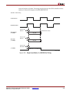
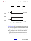
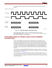
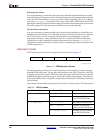
Figure 3-28 and Figure 3-29 show two store operations with variable latency for single-
cycle mode and for multi-cycle mode with a CPMC405CLOCK:BRAMDSOCMCLK ratio
of 2:1.
In both single-cycle mode and multi-cycle mode, the access consists of the following
sequence:
1. The CPU launches the store request to the OCM controller.
2. The OCM controller translates the CPU order, routes address and write data, and
asserts all of the necessary output control signals.
Note: Write control signals (DSOCMWRADDRVALID, DSOCMBRAMEN,
DSOCMBRAMBYTEWRITE) are active for only one BRAMDSOCMCLK cycle and must be
registered in the FPGA fabric if they are required for further processing.
Note: DSOCMBRAMBYTEWRITE indicates a valid write address and write data on the
DSOCMWRABUS. The DSOCMBRAMEN is also asserted for both read or write requests.
However, one can choose to ignore this signal if the design does not use BRAMs.
3. The slave waits for multiple BRAMDSOCMCLK cycles (the number of clock cycles
depends on the application) and then asserts DSOCMRWCOMPLETE, which signifies
a completion of write data store.
4. The DSOCM controller sees the completion signal (DSOCMRWCOMPLETE) and
allows the internal state machine to move forward for the next request on the DSOCM
bus.
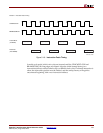
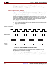
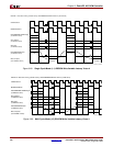
Figure 3-27: Multi Cycle Mode (2:1) DSOCM Read Variable Latency Virtex-4
UG018_63c_112103
C
PMC405Clock
D
SOCM 2:1 Data Store Timing (Variable latency, DSOCMRDWRCOMPLETE driven by OCM slaves)
B
RAMDSOCMCLK
R
ead Complete
(
From BRAM or Slave)
L
oad Address
(
To BRAM or Slave)
R
ead Data
(
To BRAM or Slave)
L_addr_1 L_addr_2
Rd_data_1 Rd_data_2
Read addr
valid
rd addr
next valid
complete complete
B
oth DSOCMBRAMEN and
D
SOCMRDADDRVALID
a
s rd addr valid
(
To BRAM or Slave)