


PowerPC™ 405 Processor Block Reference Guide www.xilinx.com 59
UG018 (v2.0) August 20, 2004 1-800-255-7778
R
Following reset, the processor block prevents the ICU from fetching instructions until the
busy signal is deasserted for the first time. This is useful in situations where the processor
block is reset by a core reset, but PLB devices are not reset. Waiting for the busy signal to be
deasserted prevents fetch requests following reset from interfering with PLB activity that
was initiated before reset.
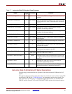
PLBC405ICUERR (Input)
When asserted, this signal indicates the PLB slave detected an error when attempting to
access or transfer the instructions requested by the ICU. This signal should be asserted
with the read-data acknowledgement signal that corresponds to the erroneous transfer.
The error signal should be asserted for only one cycle. When deasserted, no error is
detected.
If a cacheable instruction is transferred with an error indication, it is loaded into the ICU fill
buffer. However, the cache line held in the fill buffer is not transferred to the instruction
cache.
The PLB slave must not terminate instruction transfers when an error is detected. The
processor block is responsible for responding to any error detected by the PLB slave. A
machine-check exception occurs if the PowerPC 405 attempts to execute an instruction that
was transferred to the ICU with an error indication. If an instruction is transferred with an
error indication but is never executed, no machine-check exception occurs.
The PLB slave should latch error information in DCRs so that software diagnostic routines
can attempt to report and recover from the error. A bus-error address register (BEAR)
should be implemented for storing the address of the access that caused the error. A bus-
error syndrome register (BESR) should be implemented for storing information about
cause of the error.
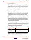
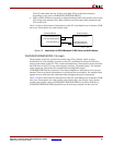
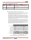
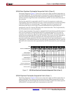
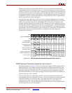
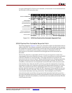
Instruction-Side PLB Interface Timing Diagrams
The following timing diagrams show typical transfers that can occur on the ISPLB interface
between the ICU and a bus-interface unit (BIU). These timing diagrams represent the
optimal timing relationships supported by the processor block. The BIU can be
implemented using the FPGA processor local bus (PLB) or using customized hardware.
Not all BIU implementations support these optimal timing relationships.
The ICU only performs reads (fetches) when accessing instructions across the ISPLB
interface.
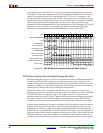
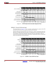
ISPLB Timing Diagram Assumptions
The following assumptions and simplifications were made in producing the optimal
timing relationships shown in the timing diagrams:
x Fetch requests are acknowledged by the BIU in the same cycle they are presented by
the ICU. This represents the earliest cycle a BIU can acknowledge a fetch request.
x The first read-data acknowledgement for a line transfer is asserted in the cycle
immediately following the fetch-request acknowledgement. This represents the
earliest cycle a BIU can begin transferring instructions to the ICU in response to a
fetch request. However, the earliest the FPGA PLB begins transferring instructions is
two cycles after the fetch request is acknowledged.
x Subsequent read-data acknowledgements for a line transfer are asserted in the cycle
immediately following the prior read-data acknowledgement. This represents the