


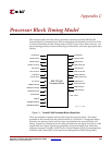
PowerPC™ 405 Processor Block Reference Guide www.xilinx.com 221
UG018 (v2.0) August 20, 2004 1-800-255-7778
R
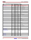
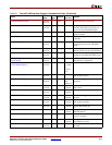
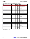
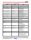
PLBC405DCUWRDACK (INPUT) V-II Pro
and V-4
I DSPLB 0 Indicates the data on the DCU write-
data bus is being accepted by the PLB
slave.
PLBC405ICUADDRACK (INPUT) V-II Pro
and V-4
I ISPLB 0 Indicates a PLB slave acknowledges
the current ICU fetch request.
PLBC405ICUBUSY (INPUT) V-II Pro
and V-4
I ISPLB 0 Indicates the PLB slave is busy
performing an operation requested by
the ICU.
PLBC405ICUERR (INPUT) V-II Pro
and V-4
I ISPLB 0 Indicates an error was detected by the
PLB slave during the transfer of
instructions to the ICU.
PLBC405ICURDDACK (INPUT) V-II Pro
and V-4
I ISPLB 0 Indicates the ICU read-data bus
contains valid instructions for transfer
to the ICU.
PLBC405DCURDDBUS[0:63] V-II Pro
and V-4
I ISPLB The ICU read-data bus used to transfer
instructions from the PLB slave to the
ICU.
PLBC405ICURDWDADDR[1:3] (INPUT) V-II Pro
and V-4
I ISPLB 0 Indicates which word or doubleword
of a four-word or eight-word line
transfer is present on the ICU read-
data bus.
PLBC405ICUSSIZE1 (INPUT) V-II Pro
and V-4
I ISPLB 0 Specifies the bus width (size) of the
PLB slave that accepted the request.
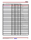
PLBCLK (INPUT) V-II Pro
and V-4
IFPGA1
Required
PLB clock.
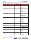
RSTC405RESETCHIP (INPUT) V-II Pro
and V-4
IReset0
Required
Indicates a chip-reset occurred.
RSTC405RESETCORE (INPUT) V-II Pro
and V-4
IReset0
Required
Resets the PowerPC 405 core logic,
data cache, instruction cache, and the
on-chip memory controller (OCM).
RSTC405RESETSYS (INPUT) V-II Pro
and V-4
IReset0
Required
Indicates a system-reset occurred.
Resets the logic in the PowerPC 405
JTAG unit.
TIEAPUCONTROL[0:15] V-4 I FCM 0 Reset values for the APU control
register.
TIEAPUUDI1[0:23] V-4 I FCM 0 Reset value for UDI register 1.
TIEAPUUDI2[0:23] V-4 I FCM 0 Reset value for UDI register 2.
TIEAPUUDI3[0:23] V-4 I FCM 0 Reset value for UDI register 3.
TIEAPUUDI4[0:23] V-4 I FCM 0 Reset value for UDI register 4.
TIEAPUUDI5[0:23] V-4 I FCM 0 Reset value for UDI register 5.
TIEAPUUDI6[0:23] V-4 I FCM 0 Reset value for UDI register 6.
TIEAPUUDI7[0:23] V-4 I FCM 0 Reset value for UDI register 7.
TIEAPUUDI8[0:23] V-4 I FCM 0 Reset value for UDI register 8.
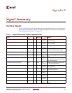
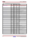
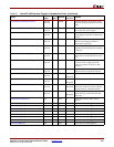
Table B-1: PowerPC 405 Interface Signals in Alphabetical Order (Continued)
Signal
FPGA
Type
a
I/O
Type
Interface
If Unused
Ties To:
b
Function