


88 www.xilinx.com PowerPC™ 405 Processor Block Reference Guide
1-800-255-7778 UG018 (v2.0) August 20, 2004
Chapter 2: Input/Output Interfaces
R
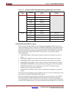
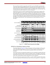
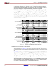
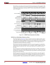
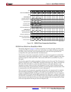
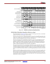
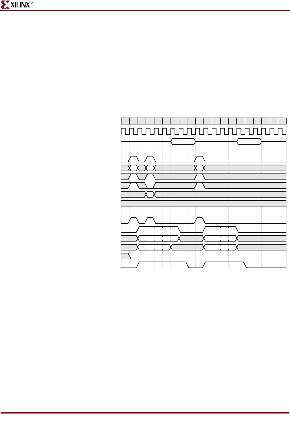
is sent from the BIU to the DCU fill buffer in cycle 7. The DCU uses the byte enables to
select the appropriate bytes from the read-data bus. The data is not cacheable, so the fill
buffer is not transferred to the data cache after this transaction is completed.
The third line read (rl3) cannot be requested until the first request (rl1) is complete. The
earliest this request can occur is in cycle 7. However, the request is delayed to cycle 10
because the DCU is busy transferring the fill buffer to the data cache in cycles 7 through 9
(fill1). The BIU can respond immediately to the rl3 request because all transactions
associated with the second request (rw2) are complete. Data is sent from the BIU to the
DCU fill buffer in cycles 11 through 14. After all data associated with this line is read, it is
transferred by the DCU from the fill buffer to the data cache. This is represented by the fill3
transaction in cycles 15 through 17.
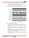
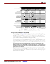
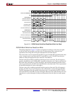
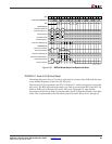
DSPLB Three Consecutive Word Reads
The timing diagram in Figure 2-19 shows three consecutive word reads. The word reads
could be in response to non-cacheable loads or cacheable loads that do not allocate a cache
line.
Figure 2-19 provides an example of the fastest speed at which the PowerPC 405 DCU can
request and receive single words over the PLB. The DCU is designed to wait for the current
single-word read request to be satisfied before making a subsequent request. This
requirement results in the delay between requests shown in the figure. It is possible for
other PLB masters to request and receive single words at a faster rate than shown in this
example.
The first word read (rw1) is requested by the DCU in cycle 2 and the BIU responds in the
same cycle. A single word is sent from the BIU to the DCU in cycle 3. The DCU uses the
byte enables to select the appropriate bytes from the read-data bus.
Figure 2-18: DSPLB Line Read/Word Read/Line Read
Cy cle
1 2 3 4 5 6 7 8 9 10 11 12 13 14 15 16 17 18 19 20
PLBCLK and CPMC405CLK
UG018_22_101701
PPC405 Outputs:
C405PLBDCUREQUEST
C405PLBDCURNW
C405PLBDCUABUS[0:31]
adr1 adr2
val
adr3
fill1 fill3
C405PLBDCUBE[0:7]
C405PLBDCUWRDBUS[0:63]
C405PLBDCUSIZE2
DCU
rw2 rl3rl1
PLB/BIU Outputs:
PLBC405DCUADDRACK
PLBC405DCURDDBUS[0:63]
PLBC405DCURDWDADDR[1:3]
PLBC405DCURDDACK
PLBC405DCUWRDACK
PLBC405DCUBUSY
rw2 rl3rl1
rl1
01
rl1
23
rl1
45
rl1
67
rw2 rl3
01
rl3
23
rl3
45
rl3
67
d1
01
d1
23
d1
45
d1
67
d2 d3
01
d3
23
d3
45
d3
67
0246 0246