


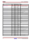
PowerPC™ 405 Processor Block Reference Guide www.xilinx.com 217
UG018 (v2.0) August 20, 2004 1-800-255-7778
R
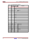
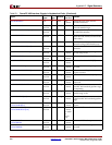
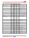
CPMC405TIMERCLKEN V-II Pro
and V-4
I CPM 1 Enables the timer clock zone.
CPMC405TIMERTICK V-II Pro
and V-4
I CPM 1 Increments or decrements the
PowerPC 405 timers every time it is
active with the CPMC405CLOCK.
CPMDCRCLK V-4 I CPM 1 DCR bus interface clock for PPC405
synchronization.
CPMFCMCLK V-4 I CPM 1 FCM interface clock for the APU
Controller.
DBGC405DEBUGHALT V-II Pro
and V-4
I Debug 0 Indicates the external debug logic is
placing the processor in debug halt
mode.
DBGC405EXTBUSHOLDACK V-II Pro
and V-4
I Debug 0 Indicates the bus controller has given
control of the bus to an external master.
DBGC405UNCONDDEBUGEVENT V-II Pro
and V-4
I Debug 0 Indicates the external debug logic is
causing an unconditional debug event.
DCRC405ACK
EXTDCRACK
V-II Pro
and V-4
I DCR 0 Indicates a DCR access has been
completed by a peripheral.
DCRC405DBUSIN[0:31]
EXTDCRDBUSIN[0:31]
V-II Pro
and V-4
IDCR0
or attach
to
output
bus
The 32-bit DCR read-data bus.
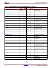
DSARCVALUE[0:7] V-II Pro
and V-4
I DSOCM 0 Power-on base address for the data-
side on-chip memory
DSCNTLVALUE[0:7] V-II Pro
and V-4
IDSOCMBit 3=1
All
others=0
Power-on configuration of the DSOCM
controller
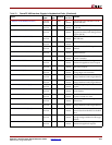
DSOCMBRAMABUS[8:29] V-II Pro
and V-4
ODSOCMNo
Connect
Address from the DSOCM controller to
FPGA fabric
DSOCMBRAMBYTEWRITE[0:3] V-II Pro
and V-4
ODSOCMNo
Connect
Indicates a write access
DSOCMBRAMEN V-II Pro
and V-4
ODSOCMNo
Connect
BRAM enable signal asserted on
accesses
DSOCMBRAMWRDBUS[0:31] V-II Pro
and V-4
ODSOCMNo
Connect
Write data from DSOCM to the data-
side memory interface
DSOCMBUSY V-II Pro
and V-4
ODSOCMNo
Connect
Value of the DSOCM DCR control
register DSCNTL[2] bit
DSOCMWRADDRVALID V-4 O DSOCM No
Connect
The signal indicates a valid read access
and read address
DSOCMRWCOMPLETE V-4 I DSOCM 0 Indicates that a read access or a write
access is complete
DSOCMWRADDRVALID V-4 O DSOCM No
Connect
The signal indicates a write and that
write address is valid
EICC405CRITINPUTIRQ V-II Pro
and V-4
I EIC 0 Indicates an external critical interrupt
occurred.
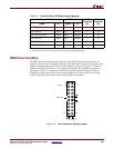
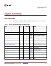
Table B-1: PowerPC 405 Interface Signals in Alphabetical Order (Continued)
Signal
FPGA
Type
a
I/O
Type
Interface
If Unused
Ties To:
b
Function