


PowerPC™ 405 Processor Block Reference Guide www.xilinx.com 43
UG018 (v2.0) August 20, 2004 1-800-255-7778
R
instructions following the load require the loaded data. Disabling operand forwarding
may improve the performance (clock frequency) of the PowerPC 405.
C405XXXMACHINECHECK (Output)
When asserted, this signal indicates the PowerPC 405 detected an instruction machine-
check error. When deasserted, no error exists. This signal is asserted when the processor
attempts to execute an instruction that was transferred to the PowerPC 405 with the
PLBC405ICUERR signal asserted. This signal remains asserted until software clears the
instruction machine-check bit in the exception-syndrome register (ESR[MCI]).
Reset Interface
A reset causes the processor block to perform a hardware initialization. It always occurs
when the processor block is powered up and can occur at any time during normal
operation. If it occurs during normal operation, instruction execution is immediately
halted and all processor state is lost.
The processor block recognizes three types of reset:
x A processor reset affects only the processor block, including PowerPC 405 execution
units, cache units, the device control register controller (DCR), and the on-chip
memory controller (OCM). On Virtex-4-FX, it also resets the auxiliary processor unit
controller (APU). External devices (on-chip and off-chip) are not affected. This type of
reset is also referred to as a core reset.
x A chip reset affects the processor block and all other devices or peripherals located on
the same chip as the processor.
x A system reset affects the processor chip and all other devices or peripherals external to
the processor chip that are connected to the same system-reset network. The scope of
a system reset depends on the system implementation. Power-on reset (POR) is a form
of system reset.
Input signals are provided to the processor block for each reset type. The signals are used
to reset the processor block and to record the reset type in the debug-status register
(DBSR[MRR]). The processor block can produce reset-request output signals for each reset
type. External reset logic can process these output signals and generate the appropriate
reset input signals to the processor block. Reset activity does not occur when the processor
block requests the reset. Reset activity occurs only when external logic asserts the
appropriate reset input signal.
Reset Requirements
FPGA logic (external to the processor block) is required to generate the reset input signals
to the processor block. The reset input signals can be based on the reset-request output
signals from the processor block, system-specific reset-request logic, or a combination of
the two. Reset input signals must meet the following minimum requirements:
x The reset input signals must be synchronized with the PowerPC 405 clock.
x The reset input signals must be asserted for at least eight (CPMC405CLOCK) clock
cycles.
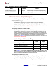
x Only the combinations of signals shown in Table 2-5 are used to cause a reset.
POR (power-on reset) is handled by logic within the processor block. This logic asserts the
RSTC405RESETCORE, RSTC405RESETCHIP, RSTC405RESETSYS, and