


PowerPC™ 405 Processor Block Reference Guide www.xilinx.com 167
UG018 (v2.0) August 20, 2004 1-800-255-7778
R
DCR Read Access
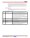
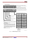
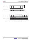
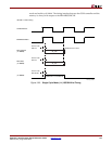
If the ISINIT register is read back on the DCR:
x For Virtex-II Pro, bits A8-A29 are mapped onto DCR read data bus bits D0-D21 as
shown in Figure 3-16, please note that the mapping for read access is different from
write.
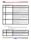
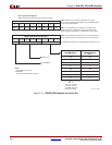
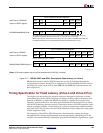
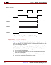
x For Virtex-4, if bit 2 of ISENTL is set to 1, bits A8-A29 are mapped onto DCR read bus
bits D8-D29, as shown in Figure 3-17. This helps to eliminate bit shifting in software
for further operation on the DCR read value of the ISINIT register. The read address
on the memory interface is A8 to A28. Address bit A29 is used to control the
ISOCMDCRBRAMEVENEN and ISOCMDCRBRAMODDEN signals. Each time
register ISFILL is written, there is one 32-bit instruction written into the BRAM (odd
or even, depending on the value of address bit A29). Otherwise, if bit 2 of ISCNTL is
set to 0, ISINIT is mapped the same way as it is in Virtex-II Pro during DCR read.
If the ISFILL register is read back on the DCR:
x For Virtex-II Pro, the current content stored in the ISFILL register will be returned as
DCR read data. The actual content of ISOCM addressed by the ISINIT register will not
be loaded.
x For Virtex-4, if the DCR-Based Read Back feature is enabled (bit 2 of ISCNTL in
Virtex-4 is set to 1), the actual content of ISOCM addressed by ISINIT register will be
loaded, otherwise, the current content stored in the ISFILL register will be returned as
DCR read data.