


PowerPC™ 405 Processor Block Reference Guide www.xilinx.com 173
UG018 (v2.0) August 20, 2004 1-800-255-7778
R
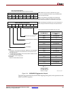
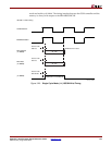
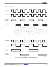
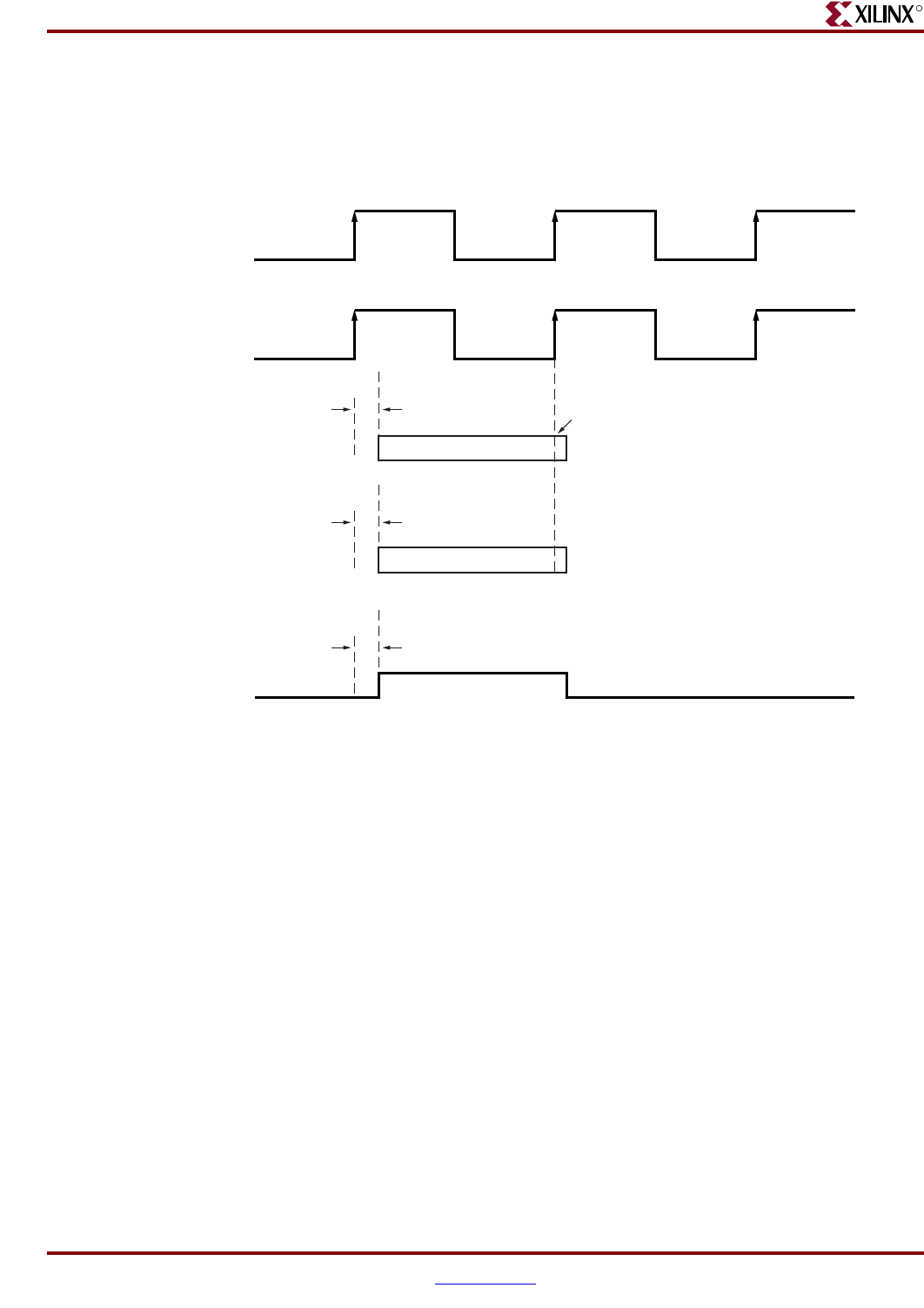
mode and multi-cycle Mode. The timing interface between the OCM controller and the
memory is always with respect to the BRAMISOCMCLK.
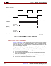
Figure 3-20: Single Cycle Mode (1:1) ISOCM Write Timing
UG018_66_03060
3
C
PMC405Clock
I
SOCM 1:1 Write Timing
B
RAMISOCMCLK
W
rite Address
(
To BRAM)
Clock to Valid
Addr Out
W
rite Data
(
To BRAM)
W_addr
BRAM latches in data
W_data
(
To BRAM)
OddWriteEn or EvenWriteEn
Clock to Valid
Data Out
Clock to Valid
Write Enable