


PowerPC™ 405 Processor Block Reference Guide www.xilinx.com 193
UG018 (v2.0) August 20, 2004 1-800-255-7778
R
The reset value of the individual UDI registers can be defined using attribute inputs to the
APU Controller. For details see the “APU Controller Attributes” section in this chapter.
DCR Access to the Configuration Registers
The APU Controller general configuration register has its own DCR address and can be
read and written using normal DCR accesses. Refer to the section “Internal Device Control
Register (DCR) Interface” in Chapter 2 for address mapping.
The eight UDI registers share a single DCR address for accessing. A UDI register pointer
allows individual access to the different registers.
When performing a DCR write to the UDI configuration register address, the DCRRegPtr
field of the write data is used to select which UDI register to write, that is, if DCRRegPtr=3,
then the DCR write will affect the configuration register associated with UDI number 3.
For this DCR write operation, the Type filed should be one of the following: autonomous,
blocking or non-blocking.
A DCR read from the UDI configuration register address uses a 3-bit read pointer register
in the APU Controller to select which specific UDI configuration to return. This pointer
auto-increments after each DCR read operation. To load the read pointer with a specific
value, the user must perform a “ghost” write to the UDI configuration DCR address. This
write will not affect the contents of any UDI configuration registers, only the read pointer.
The data used for a “ghost” write has two significant fields: the Type field and the
DCRRegPtr field. All other data fields are ignored. The Type field must be set to 0b11, and
the DCRRegPtr should be set to the desired read pointer value. A DCR read performed to
the UDI configuration address after such “ghost” write will return the contents of the
desired UDI configuration register.
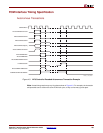
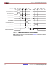
Interface Definition
The tables below describe all I/O ports related to the APU Controller. They connect the
APU Controller in the PowerPC 405 block to the FCM in the FPGA fabric. The naming
convention implies the direction of the data flow: “APUFCM” signifies “from APU
Controller to FCM”, and “FCMAPU” represents “from FCM to APU Controller” .
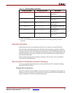
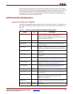
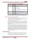
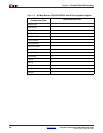
- (21:25) Hard coded 0b0000.
Type (26:27) Instruction class definition, and reserved DCR use:
0b00 = Blocking
0b01 = Non-blocking
0b10 = Autonomous
0b11 = reserved for UDI register selection for DCR read
operations (see “DCR Access to the Configuration
Registers”).
DCRRegPtr (28:30) reserved for DCR UDI register addressing (see “DCR
Access to the Configuration Registers”)
UDIEn 31 Enable APU Controller decoding of this UDI
configuration.
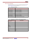
Table 4-5: UDI Configuration Register Bit Description (Continued)
Name Bit Description