


PowerPC™ 405 Processor Block Reference Guide www.xilinx.com 75
UG018 (v2.0) August 20, 2004 1-800-255-7778
R
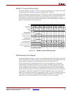
An eight-word line transfer moves the cache line aligned on the address specified by
C405PLBDCUABUS[0:26]. This cache line contains the target data accessed by the DCU.
The cache line is transferred using four doubleword or eight word transfer operations,
depending on the PLB slave bus width (64-bit or 32-bit, respectively).
The words moved during an eight-word line transfer can be sent from the PLB slave to the
DCU in any order (target-word-first, sequential, other). This transfer order is specified by
PLBC405DCURDWDADDR[1:3].
C405PLBDCUCACHEABLE (Output)
This signal indicates whether the accessed data is cacheable. It reflects the value of the
cacheability storage attribute for the target address. The data is non-cacheable when the
signal is deasserted (0). The data is cacheable when the signal is asserted (1). This signal is
valid when the DCU is presenting a data-access request to the PLB slave. The signal
remains valid until the cycle following acknowledgement of the request by the PLB slave.
(The PLB slave asserts PLBC405DCUADDRACK to acknowledge the request.)
Non-cacheable data is usually transferred as a single word. Software can indicate that non-
cacheable reads be loaded using an eight-word line transfer by setting the load-word-as-line
bit in the core-configuration register (CCR0[LWL]) to 1. This enables non-cacheable reads
to take advantage of the PLB line-transfer protocol to minimize PLB-arbitration delays and
bus delays associated with multiple, single-word transfers. The transferred data is placed
in the DCU fill buffer, but not in the data cache. Subsequent data reads from the same non-
cacheable line are read from the fill buffer instead of requiring a separate arbitration and
transfer sequence across the PLB. Data in the fill buffer are read with the same performance
as a cache hit. The non-cacheable line remains in the fill buffer until the fill buffer is needed
by another line transfer.
Cacheable data is transferred as a single word or as an eight-word line, depending on
whether the transfer allocates a cache line. Transfers that allocate cache lines use an eight-
word transfer size. Transfers that do not allocate cache lines use a single-word transfer size.
Line allocation of cacheable data is controlled by the core-configuration register. The load
without allocate bit CCR0[LWOA] controls line allocation for cacheable loads and the store
without allocate bit CCR0[SWOA] controls line allocation for cacheable stores. Clearing the
appropriate bit to 0 enables line allocation (this is the default) and setting the bit to 1
disables line allocation. The dcbt and dcbtst instructions always allocate a cache line and
ignore the CCR0 bits.
C405PLBDCUWRITETHRU (Output)
This signal indicates whether the accessed data is in write-through or write-back cacheable
memory. It reflects the value of the write-through storage attribute which controls the
caching policy of the target address. The data is in write-back memory when the signal is
deasserted (0). The data is in write-through memory when the signal is asserted (1). This
signal is valid when the DCU is presenting a data-access request to the PLB slave and when
the data cacheability signal is asserted. The signal remains valid until the cycle following
acknowledgement of the request by the PLB slave (the PLB slave asserts
PLBC405DCUADDRACK to acknowledge the request).
The system designer can use this signal in systems that require shared memory coherency.
Stores to write-through memory update both the data cache and system memory. Stores to
write-back memory update the data cache but not system memory. Write-back memory
locations are updated in system memory when a cache line is flushed due to a line
replacement or by executing a dcbf or dcbst instruction. See the PowerPC Processor
Reference Guide for more information on memory coherency and caching policy.