


112 www.xilinx.com PowerPC™ 405 Processor Block Reference Guide
1-800-255-7778 UG018 (v2.0) August 20, 2004
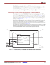
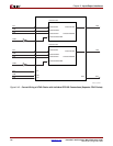
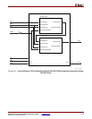
Chapter 2: Input/Output Interfaces
R
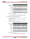
JTAG Interface I/O Signal Descriptions
The following sections describe the operation of the JTAG interface I/O signals.
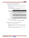
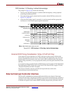
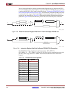
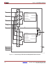
JTGC405TCK (Input)
This input is the JTAG TCK (Test ClocK) signal. The TMS and TDI signals are latched on
the rising edge of TCK, while TDO is valid on the falling edge of TCK. The maximum TCK
frequency is one-half the CPMC405CLOCK frequency.
JTGC405TMS (Input)
This input is the JTAG TMS (Test Mode Select) signal. It is latched by the processor on the
rising edge of TCK. The value of the signal is typically changed by external logic on the
falling edge of TCK. The TMS signal is used to select the next state in the TAP (JTAG) state
machine.
JTGC405TDI (Input)
This input is the JTAG TDI signal. It is latched by the processor on the rising edge of TCK.
The value of the signal is typically changed by external logic on the falling edge of TCK.
Data received on this input signal is placed into the Instruction Register or the appropriate
Data Register as specified by the TAP state machine.
JTGC405TRSTNEG (Input)
This input is the active-low JTAG test reset (TRST) signal. This signal may be either tied
high or wired to a user I/O. Note that the device does not implement the TRST signal. If
JTC405TRSTNEG is tied high, the PPC405 TAP may be reset synchronously by clocking
five 1’s on TMS. This signal is automatically used by the processor block during power-on
reset to reset the JTAG logic.
JTGC405BNDSCANTDO (Input)
This input should not be used; leave it unconnected.
C405JTGTDO (Output)
This output is the JTAG TDO (Test Data Out) signal. It is driven by the processor with a
new value on the falling edge of the JTAG clock when the PPC405 TAP is in either the Shift-
DR or Shift-IR state. The C405JTGTDO output is not valid in other TAP states.
C405JTGTDOEN (Output)
This output is asserted (logic High) when the C405JTGTDO signal is valid.
C405JTGEXTEST (Output)
This output should not be used; leave it unconnected.
C405JTGCAPTUREDR (Output)
This output is asserted (logic High) when the PPC405 TAP is in the Capture-DR state. Most
designs do not require this signal and should leave it unconnected.