174 www.xilinx.com PowerPC™ 405 Processor Block Reference Guide
1-800-255-7778 UG018 (v2.0) August 20, 2004
Chapter 3: PowerPC 405 OCM Controller
R
DSOCM Data Load, Fixed Latency
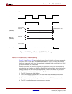
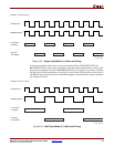
Figure 3-22 and Figure 3-23 show two back-to-back loads for single-cycle mode and multi-
cycle mode with a CPMC405CLOCK:BRAMDSOCMCLK ratio of 2:1. Note that for both
single cycle and multi-cycle mode, the maximum sustainable load completion is one load
per two BRAMDSOCMCLK periods.
In single-cycle mode, the first load requires four processor clock cycles to complete. The
processor core can launch a new address, called back-to-back operation, as soon as the first
address is latched into the OCM controller interface, which is internal to the processor
block. The initial access consists of the following sequence:
1. The CPU launches the load address.
2. The OCM controller translates the CPU order and routes the address and control
signals onto the DSOCM bus.
3. One wait state is introduced to permit the synchronous BRAM to access the data.
4. The CPU stores the data into a general-purpose register.
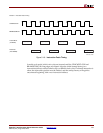
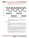
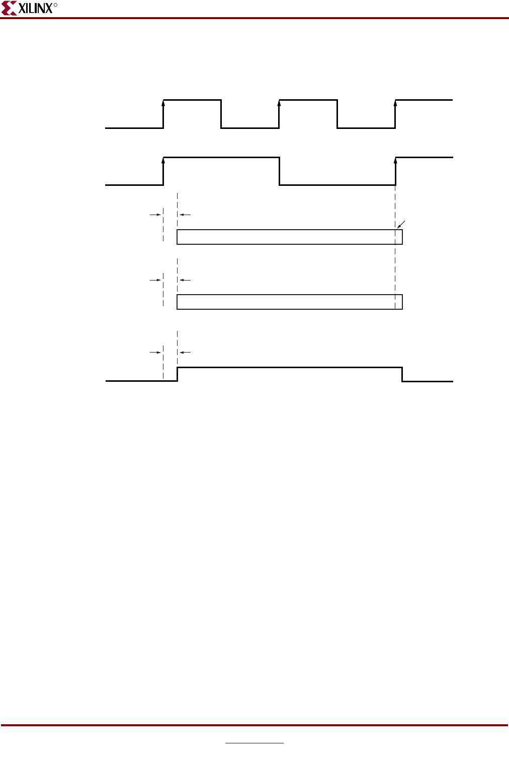
Figure 3-21: Multi Cycle Mode (2:1) ISOCM Write Timing
UG018_67_030603
C
PMC405Clock
I
SOCM 2:1 Write Timing
B
RAMISOCMCLK
W
rite Address
(
To BRAM)
Clock to Valid
Addr Out
W
rite Data
(
To BRAM)
W_addr
BRAM latches in da
ta
W_data
(
To BRAM)
OddWriteEn or EvenWriteEn
Clock to Valid
Data Out
Clock to Valid
Write Enable


