172 www.xilinx.com PowerPC™ 405 Processor Block Reference Guide
1-800-255-7778 UG018 (v2.0) August 20, 2004
Chapter 3: PowerPC 405 OCM Controller
R
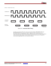
In order to estimate the theoretical maximum number of instruction fetches per second on
the OCM interface, measure the period of the BRAM clock cycle to determine the
maximum throughput.
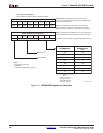
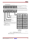
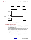
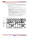
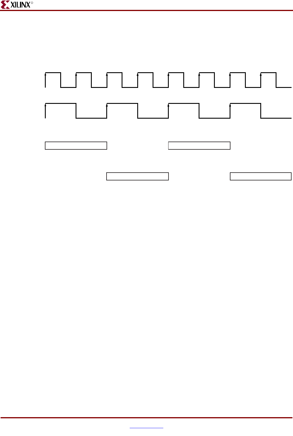
In the figures above, L_addr_n refers to the OCM controller address outputs
ISOCMBRAMRDADDR and Rd_data_n refers to the OCM controller instruction data bus
inputs BRAMISOCMRDDBUS from the ISBRAM.
Writing to ISBRAM
There are two methods used to write to the instruction side memory. Typically, the BRAM
is initialized in the device configuration bitstream. The Data2MEM software utility in the
design implementation tools is used to load BRAM with instructions as well as data. If the
application code is static, this eliminates the need to use the DCR based writes through the
ISOCM controller.
Write accesses to the ISOCM-attached memory can be performed using the DCR bus. The
DCR ISINIT register is first initialized with a start address, then every DCR write to the
ISFILL register results in a write into BRAM. The least significant bit of the ISINIT register
is used to control the initial state of the odd and even write enable outputs of the ISOCM.
Every write to the ISFILL register causes the ISOCMBRAMEVENWRITEEN and
ISOCMBRAMODDWRITEEN processor block outputs to toggle. The BRAMISOCMCLK
clock is the same for both read and write operations.
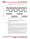
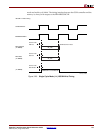
All of the read and write interface signals must be included in determining the maximum
frequency of operation for the OCM interface. These signals include write address, write
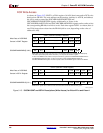
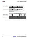
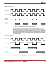
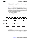
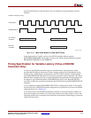
data, read address, read data and write enable interface signals. Figure 3-20 and
Figure 3-21 show the timing diagrams for a write to instruction memory in single-cycle
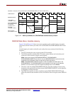
Figure 3-19: Multi-Cycle Mode (2:1) Instruction Fetch Timing
UG018_61_03060
3
C
PMC405Clock
I
SOCM 2:1 Instruction Fetch Timing
B
RAMISOCMCLK
L
oad Address
(
To BRAM)
R
ead Data
(
From BRAM)
L_addr_1 L_addr_2
Rd_data_1 Rd_data_2


