


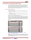
PowerPC™ 405 Processor Block Reference Guide www.xilinx.com 95
UG018 (v2.0) August 20, 2004 1-800-255-7778
R
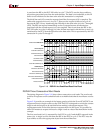
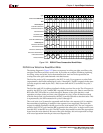
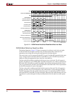
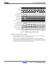
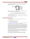
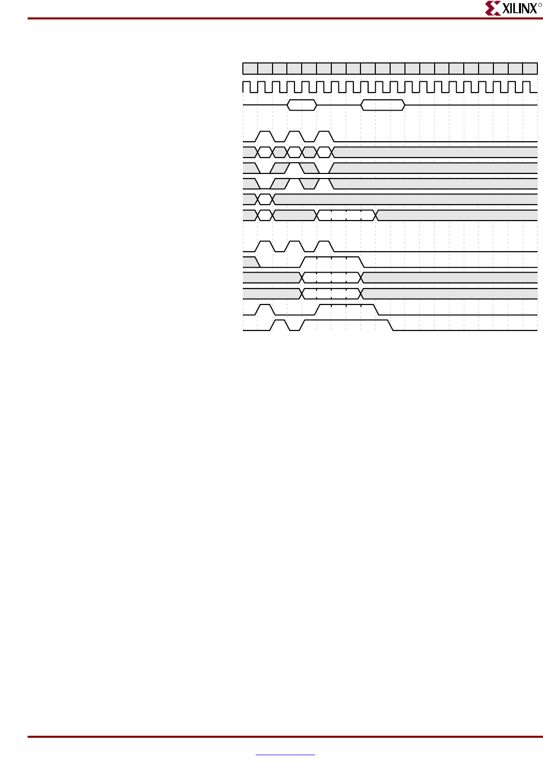
DSPLB 2:1 Core-to-PLB Line Read
The timing diagram in Figure 2-26 shows a line read in a system with a PLB clock that runs
at one half the frequency of the PowerPC 405 clock.
The line read (rl1) is requested by the DCU in PLB cycle 2, which corresponds to PowerPC
405 cycle 3. The BIU responds in the same cycle. Data is sent from the BIU to the DCU fill
buffer in PLB cycles 3 through 6 (PowerPC 405 cycles 5 through 12). After all data
associated with this line is read, it is transferred by the DCU from the fill buffer to the data
cache. This is represented by the fill1 transaction in PowerPC 405 cycles 13 through 15.
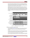
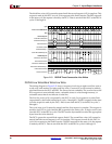
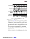
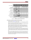
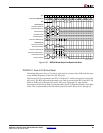
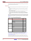
Figure 2-25: DSPLB Word Write/Line Read/Line Write
Cy cle
1 2 3 4 5 6 7 8 9 10 11 12 13 14 15 16 17 18 19 20
PLBCLK and CPMC405CLK
UG018_29_101701
PPC405 Outputs:
C405PLBDCUREQUEST
C405PLBDCURNW
C405PLBDCUABUS[0:31]
adr1 adr2 adr3
val
d1
C405PLBDCUBE[0:7]
C405PLBDCUWRDBUS[0:63]
C405PLBDCUSIZE2
PLB/BIU Outputs:
PLBC405DCUADDRACK
PLBC405DCURDDBUS[0:63]
PLBC405DCURDWDADDR[1:3]
PLBC405DCURDDACK
PLBC405DCUWRDACK
PLBC405DCUBUSY
DCU
ww1
rl2ww1 wl3
rl2ww1 wl3
rl2
01
rl2
23
rl2
45
rl2
67
wl3
01
wl3
23
wl3
45
wl3
67
d2
01
d2
23
d2
45
d2
67
d3
01
d3
23
d3
45
d3
67
0246
flush3 fill2