


PowerPC™ 405 Processor Block Reference Guide www.xilinx.com 115
UG018 (v2.0) August 20, 2004 1-800-255-7778
R
The PPC405 cores do not have their own BSDL files; instead, the necessary
INSTRUCTION_OPCODES and other information are incorporated in the device BSDL
file. The PPC405 cores are not available for interconnect tests (i.e., EXTEST,
SAMPLE/PRELOAD), as they do not have a boundary scan register. All device boundary
scan tests are performed through the FPGA boundary scan register.
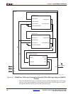
Connecting PPC405 JTAG Logic Directly to Programmable I/O
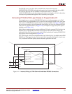
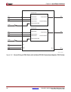
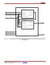
The simplest way to access the PPC405 JTAG logic is to wire the processor core’s JTAG
signals directly to programmable I/O. For devices with multiple PPC405 cores, users may
wire each set of PPC405 JTAG signals directly to programmable I/O (Figure 2-42); chain
the processors together with programmable interconnect and wire the combined PPC405
JTAG chain to programmable I/O (Figure 2-43) or multiplex a single set of JTAG pins to
multiple cores (Figure 2-44).
Each of these connection styles requires additional I/O and a separate JTAG chain for the
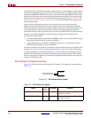
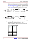
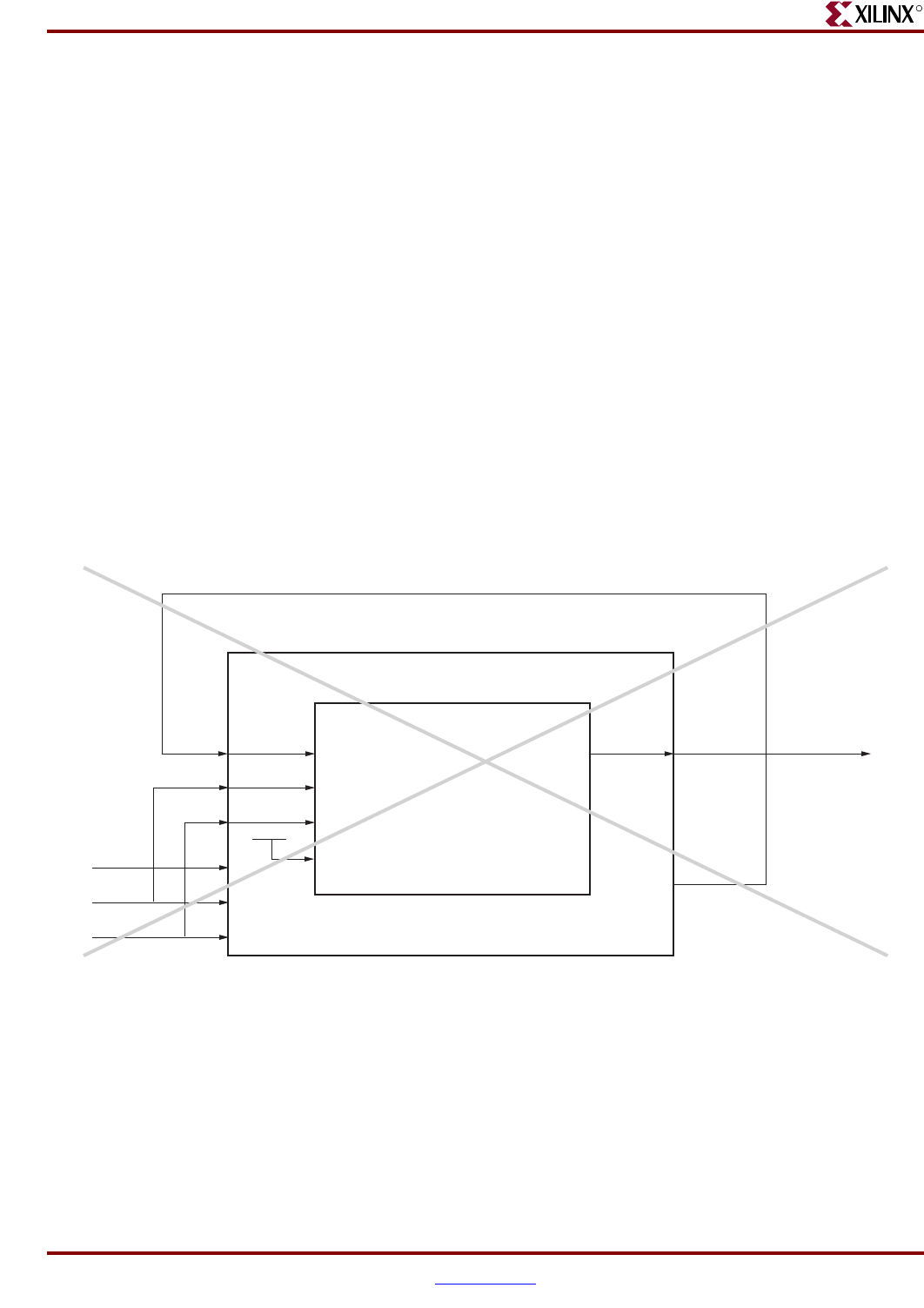
PPC405 core(s). The PPC405 cores must not be placed in the same JTAG chain as the
dedicated device JTAG pins because the chain will be broken by the missing PPC405 JTAG
logic prior to FPGA configuration (Figure 2-41).
The /TRST signal, which is not implemented on any Xilinx devices, is available on the IBM
PPC405 core. This signal may be wired to user I/O or internally tied high. If wired to user
I/O, an external 10 KOhm pullup resistor should be placed on the trace.
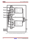
Figure 2-41: Incorrect Wiring of JTAG Chain with Individual PPC405 Connections
PPC405 Core
JTGC405TDI
C405JTGTDO
JTGC405TMS
TDO
TDO
JTGC405TCK
C405JTGTDOEN
JTGC405TRSTNEG
UG018_76_032504
TDI
TMS
TCK
TDI
TMS
TCK