


142 www.xilinx.com PowerPC™ 405 Processor Block Reference Guide
1-800-255-7778 UG018 (v2.0) August 20, 2004
Chapter 3: PowerPC 405 OCM Controller
R
OCM Controller Operation
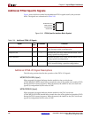
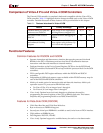
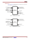
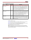
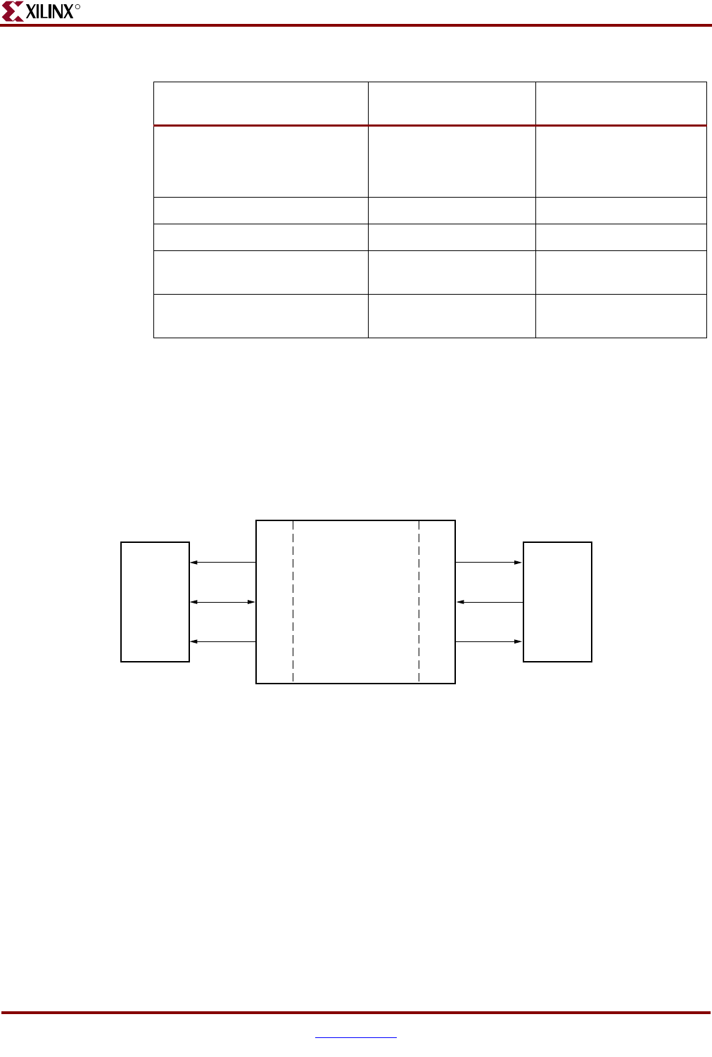
The OCM controller is distributed into two blocks, one for the ISOCM interface and the
other for the DSOCM interface, as shown in Figure 3-1.
The DSOCM and ISOCM interfaces are designed to operate independently of each other.
This provides the following advantages:
x The overall efficiency of the core is improved by eliminating the need for OCM
arbitration between two sets of operations, that is, loads and stores on the data-side
interface and instruction fetches on the instruction-side interface.
x Overall controller performance is improved because there is no need to share a
common address and data bus between the instruction-side and data-side interfaces
to the block RAM.
x Having two separate interfaces allows selection of either one or both interfaces as
required by the specific application.
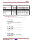
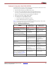
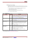
x The two control registers: DSARC and ISARC, define the base addresses for the OCM
instruction-side and data-side memory spaces. The registers are initialized on power
Clock Ratio (PPC405:OCM)
Virtex-II Pro
Virtex-4
Integer: 1:1 through 4:1
1:1 through 8:1
Integer: 1:1 through 4:1
1:1 through 8:1
Clock ratio automatic detection. Virtex-4 only Virtex-4 only
Variable Latency Read/Write Virtex-4 only Not applicable
Initialize block BRAM during
FPGA device configuration.
Yes Yes
Processor access to initialize
memory in fabric.
Load and store
instructions
DCR read and write
instructions
a. 32-bit write only port for Virtex-II Pro. 32-bit read/write port for Virtex-4.
b. Refer to the section “Device-Control Register Interfaces” in Chapter 2 for more information.
Table 3-2: DSOCM and ISOCM Features (Continued)
Feature
Data-Side
OCM Interface
Instruction-Side
OCM Interface
Figure 3-1: OCM Controller Interfaces
Data Side
Memory
D
S
O
C
M
I
S
O
C
M
Instruction
Side
Memory
Processor
Block
UG018_37x_090203