


PowerPC™ 405 Processor Block Reference Guide www.xilinx.com 119
UG018 (v2.0) August 20, 2004 1-800-255-7778
R
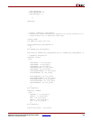
Connecting PPC405 JTAG Logic in Series with the Dedicated Device
JTAG Logic
An alternative to connecting the PPC405 JTAG logic directly to programmable I/O is to
wire it in series with the dedicated device JTAG logic. This is done by wiring the JTAG
signals on the PPC405 core to a special design element called the JTAGPPC primitive in the
user design. As described in the “JTAG Instruction Register” section above, the Instruction
Register length remains constant, regardless of how the PPC405 cores are used and
regardless of whether or not the device is configured.
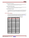
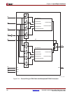
Prior to configuration, the most-significant IR bits are placed in a dummy register which is
either 4, 8, or 16 bits in length, depending on the number of available PPC405 cores in the
device (see Table 2-20). This register is used as a placeholder only. After configuration, if
the user connects the PPC405 JTAG logic in series with the dedicated device JTAG logic,
the most significant IR bits are used by the PPC405 cores. Thus, the overall IR length
remains the same for the device at all times.
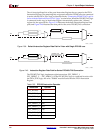
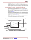
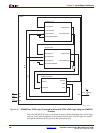
When the PPC405 JTAG logic is connected in series with the dedicated JJTAG logic, the
C405JTGTDO signal of each core is connected to the JTGC405TDI of the next. The
JTGC405TCK and JTGC405TMS signals are connected to each PPC405 core in parallel. The
C405JTGTDOEN output of each PPC405 cores must be ORed to the TDO_TS_PPC input of
the JTAGPPC primitive (for devices with only one PPC405 core, wire the C405JTGTDOEN
output directly to the TDO_TS_INPUT on the JTAGPPC primitive). The /TRST signal,
which is not implemented on the device, is implemented on the IBM PPC405 core. When
wiring the PPC405 JTAG logic in series with the FPGA JTAG logic, this signal must be
pulled High as shown in Figure 2-45.
For more information, see the appropriate Virtex-series user guide.