


PowerPC™ 405 Processor Block Reference Guide www.xilinx.com 33
UG018 (v2.0) August 20, 2004 1-800-255-7778
R
Chapter 2
Input/Output Interfaces
This chapter describes all PowerPC 405 input/output signals associated with the following
processor block interfaces:
x “Clock and Power Management Interface”
x “CPU Control Interface”
x “Reset Interface”
x “Instruction-Side Processor Local Bus Interface”
x “Data-Side Processor Local Bus Interface”
x “Device-Control Register Interfaces”
x “Internal Device Control Register (DCR) Interface”
x “External DCR Bus Interface”
x “External Interrupt Controller Interface”
x “PPC405 JTAG Debug Port”
x “Debug Interface”
x “Trace Interface”
x “Processor Version Register (PVR) Interface (Virtex-4-FX Only)”
x “Additional FPGA Specific Signals”
The sections within this chapter provide the following information:
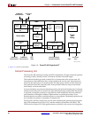
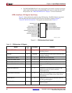
x An overview summarizing the purpose of the interface.
x An I/O symbol providing a quick view of the signal names and the direction of
information flow with respect to the processor block.
x A signal table that summarizes the function of each signal. The I/O column in these
tables specifies the direction of information flow with respect to the processor block.
x Detailed descriptions for each signal.
x Detailed timing diagrams (where appropriate) that more clearly describe the
operation of the interface. The diagrams typically illustrate best-case performance
when the core is attached to the FPGA processor local bus (PLB) core, or to custom
bus interface unit (BIU) designs.
The instruction-side and data-side OCM controller interfaces are described separately in
Chapter 3, “PowerPC 405 OCM Controller.”
The Fabric Co-Processor Module (FCM) interface associated with the Virtex-4-FX family
PowerPC 405 APU controller, is described separately in Chapter 4, “PowerPC 405 APU
Controller.”