


PowerPC™ 405 Processor Block Reference Guide www.xilinx.com 159
UG018 (v2.0) August 20, 2004 1-800-255-7778
R
locations. These bits are decoded against PPC405 address bits 0:7. These eight most
significant address bits permit the OCM controllers to reside independently in any 16 MB,
non-cacheable, memory range within the PPC405 32bit address (4 GB) memory space
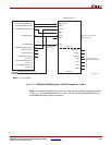
The ISOCM and DSOCM hardware outputs a maximum of 22 address bits (data-side
address bits [8:29] and instruction-side address bits [8:28]) to address memory contained in
the FPGA fabric.
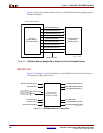
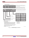
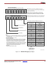
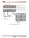
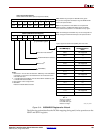
DSCNTL Registers
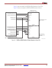
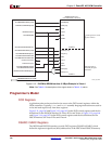
Table 3-9 and Table 3-10 describe the DSCNTL registers in Virtex-II Pro and Virtex-4
devices. For additional information, refer to Figure 3-11, page 162 (Virtex-II Pro) and
Figure 3-12, page 163 (Virtex-4).
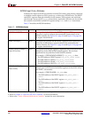
Table 3-9: DSCNTL Register for Virtex-II Pro
Bit 0 DSOCM Enable If set to 1, address decoding based on the value of DSARC will be
enabled. If set to 0, the content in DSARC will be ignored.
Bit 1 DISABLEOPERANDFWD If set to 1, load data from the DSOCM goes directly into a latch in
the processor block. This causes an additional cycle (a total of two
cycles) of latency between a load instructions which is followed by
an instruction that requires the load data as an operand.
If set to 0, load data from the DSOCM/ must pass through steering
logic before arriving at a latch. This causes a single cycle of latency
between a load instruction which is followed by an instruction that
requires the load data as an operand.
Bit 2 DSOCMBUSY This status bit can be used as a flag indicator to the FPGA fabric.
This is an optional signal.
Bit 3 Reserved. This bit must be configured to 0.
Bit 4 Reserved. This bit must be configured to 0.
Bit 5:7 DSOCMMCM CPU Clock and DSOCM Clock ratio. For Virtex-II Pro users, users
must setup the ratio in this field with valid clock ratios used in the
application system. Then the processor gasket will issue
appropriate transaction based on this ratio.