


PowerPC™ 405 Processor Block Reference Guide www.xilinx.com 153
UG018 (v2.0) August 20, 2004 1-800-255-7778
R
ISOCM Input Ports
Table 3-6 describes the Instruction Side OCM (ISOCM) input ports.
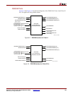
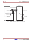
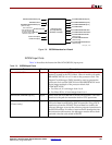
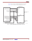
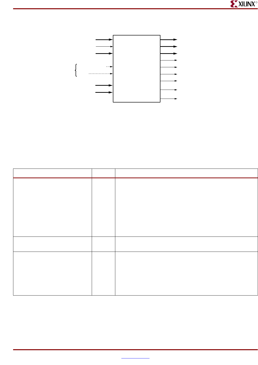
Figure 3-8: ISOCM Interface for Virtex-4
ISOCMDCRBRAMEVENEN
(Virtex-4 Only)
ISOCMDCRBRAMODDEN
(Virtex-4 Only)
UG018_38b_11210
3
RESET
ISOCMBRAMRDABUS[8:28]
BRAMISOCMRDDBUS[0:63]
B
RAMISOCMDCRRDBUS[0:31]
(
Virtex-4 Only)
ISOCMBRAMWRABUS[8:28
]
ISOCMBRAMWRDBUS[0:31
]
BRAMISOCMCLK
CPMC405CLOCK
ISCNTLVALUE[0:7]
ISARCVALUE[0:7]
ISOCMDCRBRAMRDSELEC
T
(Virtex-4 Only)
ISOCMBRAMEN
ISOCMBRAMODDWRITEEN
ISOCMBRAMEVENWRITEE
N
Clock & Reset are
same signals that go
into CPU; therefore,
no separate Clock &
Reset are required.
Instruction-Side
On-Chip Memory
(ISOCM) Controller
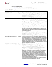
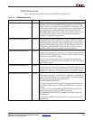
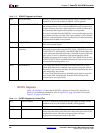
Table 3-6: ISOCM Input Ports
Port Direction Description
BRAMISOCMCLK Input This signal clocks the ISOCM controller and the instruction side
memory located in the FPGA fabric. When in multi-cycle mode,
BRAMISOCMCLK is in a 1:N ratio to the processor clock. The
Digital Clock Manager (DCM) should be used to generate the
processor clock and the ISOCM clock. BRAMISOCMCLK must
be an integer multiple of the processor block clock
CPMC405CLOCK.
x For Virtex-4, N is an integer from 1 to 8.
x For Virtex-II Pro, N is an integer from 1 to 4.
BRAMISOCMRDDBUS[0:63] Input 64-bit read data from BRAM to the ISOCM controller. The read
data bus is the path for instruction fetch of CPU operations.
BRAMISOCMDCRRDDBUS[0:31]
(Virtex-4 only)
Input
Note: Optional. Used in dual-port BRAM interface designs only.
32-bit read data from BRAM to ISOCM controller using a DCR-
based access from the PPC405. This read data bus enables the
software debugger to access the software program instructions in
the ISOCM memory. In order to insert software breakpoints into
the instruction side memory, the debugger must be able to both
read and write the code stored in BRAM.