


148 www.xilinx.com PowerPC™ 405 Processor Block Reference Guide
1-800-255-7778 UG018 (v2.0) August 20, 2004
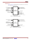
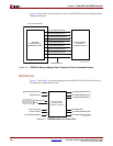
Chapter 3: PowerPC 405 OCM Controller
R
DSOCM Output Ports
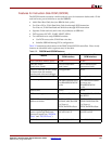
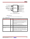
Table 3-5 describes the data-side OCM (DSOCM) output ports.
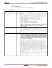
Table 3-5: DSOCM Output Ports
Port Direction Description
DSOCMBRAMEN Output This is the BRAM enable signal that is asserted for both reads and
writes to the data-side memory interface. This signal is asserted for
one and only one BRAMDSOCMCLK cycle.
DSOCMBRAMABUS[8:29] contains the address and
DSOCMBRAMWRDBUS[0:31] contains the data (for write).
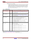
DSOCMBRAMABUS[8:29] Output Read or write address from the DSOCM controller to the data-side
FPGA fabric or memory interface. These 22 address bits
correspond to internal PPC405 address bits [8:29]. PPC405 address
bits [0:7] are compared against the DSARC register contents, and if
a match is decoded, further steps for load/store operation are
initiated.
For write accesses in both Virtex-II Pro and Virtex-4, the write
address is accompanied and qualified by a write enable signal for
each byte lane of data.
For read accesses, when the DSOCM controller is connected only
to the BRAM, DSOCMBRAMEN is asserted and must be used as a
valid address qualifier.
When the DSOCM controller is connected to a memory-mapped
slave peripheral with variable latency (Virtex-4 extended feature),
DSOCMBRAMABUS[8:29] will be qualified by the new
DSOCMRDADDRVALID signal to indicate a valid read access.
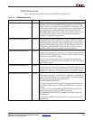
DSOCMBRAMWRDBUS[0:31] Output This bus provides 32-bit write data from the DSOCM to the data-
side memory interface. If BRAM is connected to the interface, this
port is connected directly to the data input port of the memory. For
Virtex-4 applications, this is the write data input to the memory-
mapped slave peripheral. The write data bus is further qualified
with DSOCMBRAMBYTEWRITE, and will be asserted for one and
only one BRAMDSOCMCLK cycle.
DSOCMBRAMBYTEWRITE[0:3] Output This signal indicates a write access and qualifies the
DSOCMBRAMWRDBUS. Four write enable signals support
independent byte-wide data writes into the data-side memory or
peripheral. DSOCMBRAMBYTEWRITE[0] qualifies writes to
DSOCMBRAMWRDBUS[0:7], DSOCMBRAMBYTEWRITE[1]
qualifies writes to DSOCMBRAMWRDBUS[8:15], and so on.
If the DSOCM controller is connected to memory-mapped slave
peripherals with variable latency (Virtex-4 extended feature),
DSOCMBRAMBYTEWRITE must be used as the qualification
signal for the write data bus. The signal will be asserted for one
and only one BRAMDSOCMCLK cycle. A memory-mapped slave
design should register this signal, as well as the write address and
write data (DSOCMBRAMABUS[8:29],
DSOCMBRAMWRDBUS[0:31]), if the write operation cannot be
completed in a single BRAMDSOCMCLK cycle.