


146 www.xilinx.com PowerPC™ 405 Processor Block Reference Guide
1-800-255-7778 UG018 (v2.0) August 20, 2004
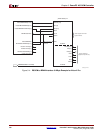
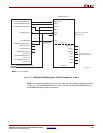
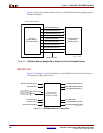
Chapter 3: PowerPC 405 OCM Controller
R
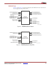
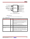
DSOCM Input Ports
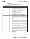
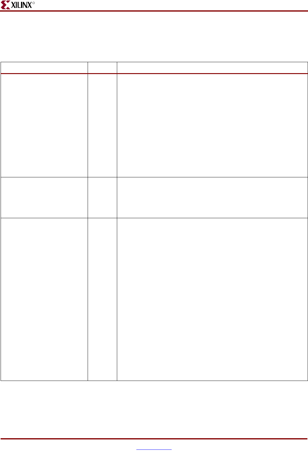
Table 3-3 describes the Data Side OCM (DSOCM) input ports.
Table 3-3: DSOCM Input Ports
Port Direction Description
BRAMDSOCMCLK Input This signal clocks the DSOCM controller and the data side interface
logic (Virtex-4 only) or memory located in the FPGA fabric. When in
multi-cycle mode, the processor clock is in an N:1 ratio with
BRAMDSOCMCLK. The frequency of BRAMDSOCMCLK must be
an integer multiple of the processor block clock input,
CPMC405CLOCK (CPU Clock). The rising edge of
BRAMDSOCMCLK must align with the rising edge of
CPMC405CLOCK.
x For Virtex-4, N is an integer from 1 to 8.
x For Virtex-II Pro, N is an integer from 1 to 4.
Note: To generate clocks with integer ratios, a Digital Clock Manager (DCM)
feature in the Virtex-II Pro and Virtex-4 fabric can be included in the
application system.
BRAMDSOCMRDDBUS[0:31] Input 32-bit read data bus from the FPGA fabric to the DSOCM controller.
For Virtex-II Pro applications, this bus originates from the read data
port of the BRAM. For Virtex-4 applications, the bus can originate
from BRAM and/or other memory-mapped peripherals located in
the fabric.
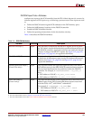
DSOCMRWCOMPLETE
(Virtex-4 only)
Input Virtex-4 supports variable latencies for the module interface with the
DSOCM controller. Virtex-4 differs from Virtex-II Pro in that a Virtex-
4 load or store operation can take an integer multiple number of BRAM
clock cycles. DSOCMRWCOMPLETE indicates that a read access or a
write access is complete. The signal should be asserted for one and only
one BRAMDSOCMCLK cycle.
For read accesses, the DSOCMRWCOMPLETE signal should be
accompanied by read data in the same clock cycle. For both read and
write operations, this signal informs the DSOCM controller in the
processor block that the current bus transaction is complete. The
DSOCM can issue the next read or write access, if required.
Unlike the CoreConnect bus architecture (PLB, OPB and DCR) there
are no complex bus protocols to handle a bus error, an abortion, or bus
timeout scenarios in this DSOCM interface. Users need to design bus
timeout logic to guarantee a fabric response to a valid DSOCM bus
cycle. If this signal is not asserted, the processor will operate
unpredictably.
Note: If you do not wish to use the variable latency feature of the Virtex-4
DSOCM and are migrating a Virtex-II Pro BRAM design, or the module that
interfaces with DSOCM controller has a fixed latency of one, this signal
should be tied to logic “1”.