


PowerPC™ 405 Processor Block Reference Guide www.xilinx.com 175
UG018 (v2.0) August 20, 2004 1-800-255-7778
R
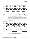
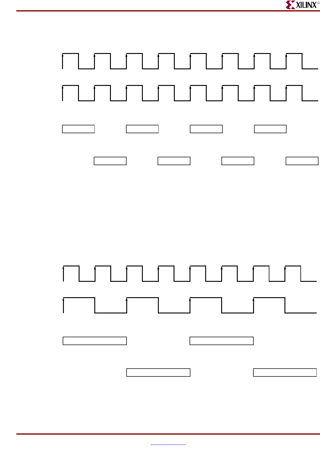
In multi-cycle mode, initial wait cycles are inserted until the CPMC405CLOCK and
BRAMDSOCMCLK rising edges are aligned. After the initial startup latency, one load (32
bits) can be completed every two BRAMDSOCMCLK clock cycles. So, in order to estimate
the theoretical maximum number of loads per second on the OCM interface, the period of
the BRAM clock should be used to establish throughput. Note that this is only an estimate
for load performance.
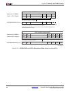
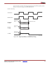
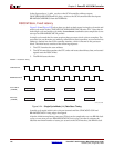
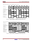
Figure 3-22: Single Cycle Mode (1:1) Data Load Timing
UG018_62_03060
3
C
PMC405Clock
DSOCM 1:1 Data Load Timing
B
RAMDSOCMCLK
L
oad Address
(
To BRAM)
R
ead Data
(
From BRAM)
L_addr_1 L_addr_2 L_addr_3 L_addr_4
Rd_data_1 Rd_data_2 Rd_data_3 Rd_data_4
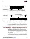
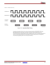
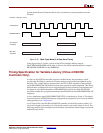
Figure 3-23: Multi Cycle Mode (2:1) Data Load Timing
UG018_63_03060
3
C
PMC405Clock
D
SOCM 2:1 Data Load Timing
B
RAMDSOCMCLK
L
oad Address
(
To BRAM)
R
ead Data
(
From BRAM)
L_addr_1 L_addr_2
Rd_data_1 Rd_data_2