


114 www.xilinx.com PowerPC™ 405 Processor Block Reference Guide
1-800-255-7778 UG018 (v2.0) August 20, 2004
Chapter 2: Input/Output Interfaces
R
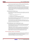
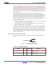
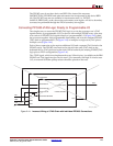
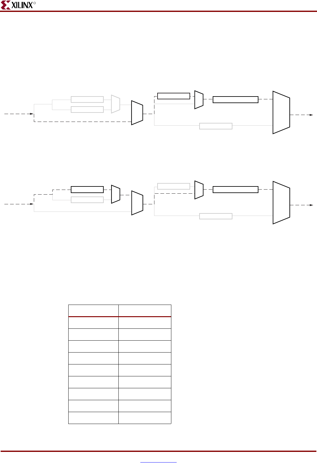
The six least significant bits of the parts Instruction Register always comprise the FPGA
Instruction Register. The remaining bits are ignored unless the PPC405 cores are connected
in series with the FPGA JTAG logic, as described in the “Connecting PPC405 JTAG Logic in
Series with the Dedicated Device JTAG Logic” section below. When the PPC405 JTAG logic
is connected in this way, its Instruction Register automatically replaces the “dummy”
register for the upper IR bits. Figure 2-39 illustrates the default Instruction Register data
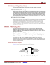
path, and Figure 2-40 illustrates the data path for the series PPC405 JTAG connection.
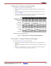
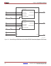
The PPC405 JTAG logic implements eight instructions: PPC_DEBUG_1,
PPC_DEBUG_2 . . . PPC_DEBUG_8. If the PPC405 JTAG logic is connected in series with
the FPGA JTAG logic, the value “100000” must be loaded into the FPGA Instruction
Register.
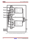
Figure 2-39: Default Instruction Register Data Path in Virtex with Single PPC405 core
TDO
TDI
FPGA DR
405 IR (3:0)
405 DR
FPGA IR (5:0)
UG018_70_100803
DUMMY (3:0)
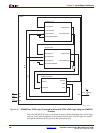
Figure 2-40: Instruction Register Data Path for Series PPC405 JTAG Connection
TDO
TDI
FPGA DR
DUMMY (3:0)
405 IR (3:0)
405 DR
FPGA IR (5:0)
UG018_71_100803
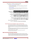
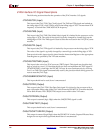
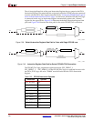
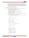
Table 2-25: PPC405 Instruction Opcodes
Instruction Opcode
PPC_BYPASS 1111
PPC_DEBUG_1 0101
PPC_DEBUG_2 0111
PPC_DEBUG_3 1001
PPC_DEBUG_4 1010
PPC_DEBUG_5 1011
PPC_DEBUG_6 1100
PPC_DEBUG_7 1101
PPC_DEBUG_8 1110