PowerPC™ 405 Processor Block Reference Guide www.xilinx.com 177
UG018 (v2.0) August 20, 2004 1-800-255-7778
R
period should be used. Note that this is only an estimate of store performance on the
interface.
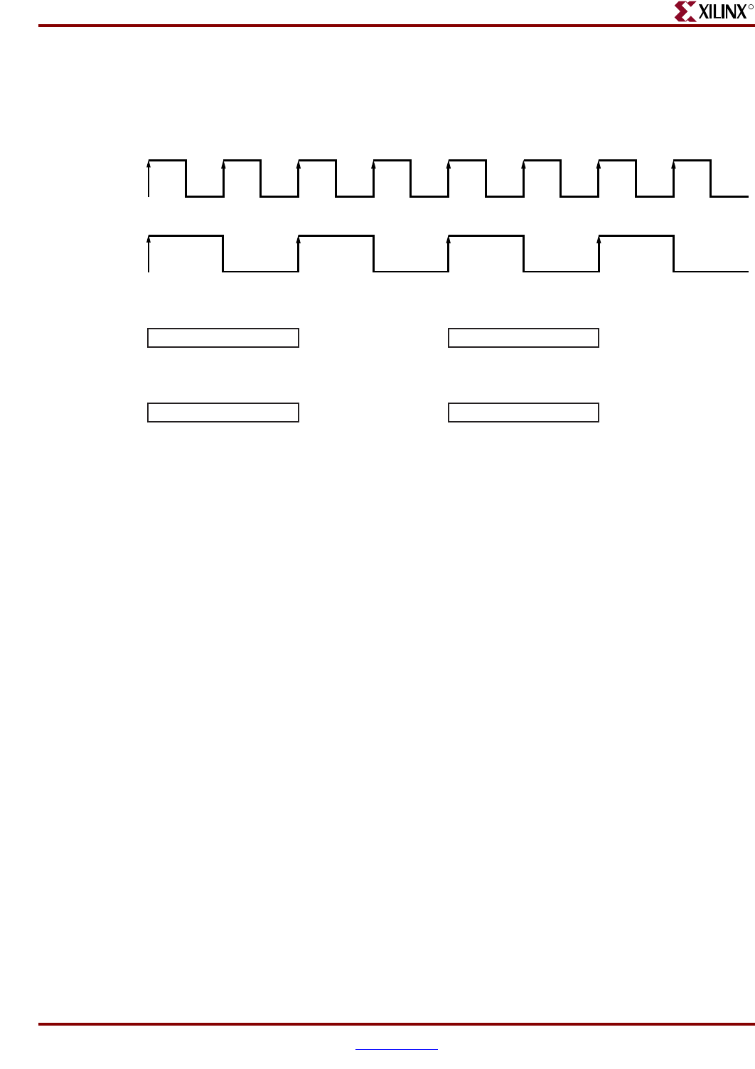
In the figures above, S_addr_n refers to the OCM controller address outputs
DSOCMBRAMWRADDR and St_data_n refers to the OCM controller data bus outputs
BRAMDSOCMWRDBUS to the DSBRAMs.
Timing Specification for Variable Latency (Virtex-4 DSOCM
Controller Only)
In Virtex-4, the DSOCM controller supports variable latency bus operations, which
provides the flexibility to attach one or more memory-mapped slave peripherals to the
interface. The variable latency feature allows the FPGA fabric interface to take multiple
clocks (BRAMDSOCMCLK) before a load or store operation can be completed. This allows
different slave peripheral devices to respond based on the application’s requirement and
not based on a pre-defined number of BRAMDSOCM clock cycles. Both the DSOCM
controller and the slave peripheral attached to the OCM still run at the BRAMDSOCMCLK
frequency.
A new completion signal, DSOCMRWCOMPLETE, is introduced in Virtex-4. This signal
must be driven by the DSOCM memory-mapped slave peripheral. For a list of use models
and applications, see “References”.
As in Virtex-II Pro, the PPC405 and DSOCM controller would still operate in either a 1:1
clock ratio (single-cycle mode) or N:1 clock ratio (multi-cycle mode, where N=2 to 8. The
following sections show examples of load and store instructions, in both single-cycle mode
and multi-cycle mode.
Figure 3-25: Multi Cycle Mode (2:1) Data Store Timing
UG018_65_040403
PMC405Clock
SOCM 2:1 Data Store Timing
RAMDSOCMCLK
tore Address
To BRAM)
rite Data
To BRAM)
S_addr_1 S_addr_2
St_data_1 St_data_2


