


40 www.xilinx.com PowerPC™ 405 Processor Block Reference Guide
1-800-255-7778 UG018 (v2.0) August 20, 2004
Chapter 2: Input/Output Interfaces
R
x PLBCLK, primary PLB I/O Bus clock.
x BRAMISOCMCLK, reference clock for the I-Side OCM controller.
x BRAMDSOCMCLK, reference clock for the D-Side OCM controller.
x CPMFCMCLK, reference clock for the APU controller (Virtex-4 only).
x CPMDCRCLK, reference clock for the external DCR bus (Virtex-4 only).
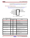
The PowerPC405 processor block supports multiple clock domains. Using several DCM
and BUFG components are recommended to create and drive the clock domains. The clock
domains include the PLB, FCM, DCR, and OCM clocks.
PLB
The PLB is used as an interface between the processor block and the higher performance
peripherals. The processor block has some internal logic to generate the appropriate
enabling signals for controlling the PLB. The PLB clock must be phased-aligned to the
processor block. All communication between the processor block and the PLB are based
upon the rising edge of the CPMC405CLOCK. The PLB is synchronous with the processor
block. The allowed supported integer clock frequency ratios between the processor block
and the PLB are 1:1, 2:1, 3:1 . . . up to 16:1. As an example, the processor block can be run at
300 MHz while the PLB bus is run at 100 MHz, in a 3:1 ratio.
DCR
The processor block clock and the DCR clock must come from the same source and be in
phase with each other. The DCR clock covers both of the processor block DCR and the
memory mapped DCR. The clock ratio between the DCR clock domain and the processor
block can run at any integer clock ratio from 1:1 to 16:1 as long as the bus transaction
completes in 64 processor block cycles. If the bus transaction does not complete in 64
processor block clock cycles, the processor block will time out and move on to the next
instruction.
Virtex-II Pro and ProX Specific
For Virtex-II Pro and Virtex-II ProX devices, there is no CPMDCRCLK input to the
processor block. Users can either set appropriate timing constraints (multi-cycle path, false
path, etc.), or simply include DCR re-synchronization logic to simply the steps to analyze
the timing related to DCR interface.
Virtex-4 Specific
For Virtex-4-FX parts there is a dedicated DCR clock input and re-synchronization registers
handling the clock boundary.
FCM (Virtex-4-FX only)
An FCM is used for highest performance integration of custom functionality defined in the
FPGA fabric with the execution pipeline of the PowerPC. The FCM clock would typically
be the same clock that clocks the FCM internally. PowerPC core to FCM interface clock
ratios can range from 1:1 to 16:1. The clocks must be rising-edge aligned.
OCM
For high speed access, the OCM clock domain covers the interface between the processor
block and the block RAM surrounding the processor block. There are two independent