


30 www.xilinx.com PowerPC™ 405 Processor Block Reference Guide
1-800-255-7778 UG018 (v2.0) August 20, 2004
Chapter 1: Introduction to the PowerPC 405 Processor
R
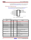
x Device control register interface
x Clock and power management interface
x JTAG port interface
x On-chip interrupt controller interface
x On-chip memory controller interface
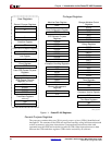
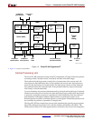
Processor Local Bus
The processor local bus (PLB) interface provides a 32-bit address and three 64-bit data buses
attached to the instruction-cache and data-cache units. Two of the 64-bit buses are attached
to the data-cache unit, one supporting read operations and the other supporting write
operations. The third 64-bit bus is attached to the instruction-cache unit to support
instruction fetching.
Device Control Register
The device control register (DCR) bus interface supports the attachment of on-chip registers
for device control. Software can access these registers using the mfdcr and mtdcr
instructions.
Clock and Power Management
The clock and power-management interface supports several methods of clock distribution
and power management.
JTAG Port
The JTAG port interface supports the attachment of external debug tools. Using the JTAG
test-access port, a debug tool can single-step the processor and examine internal-processor
state to facilitate software debugging.
On-Chip Interrupt Controller
The on-chip interrupt controller interface is an external interrupt controller that combines
asynchronous interrupt inputs from on-chip and off-chip sources and presents them to the
core using a pair of interrupt signals (critical and noncritical). Asynchronous interrupt
sources can include external signals, the JTAG and debug units, and any other on-chip
peripherals.
On-Chip Memory Controller
An on-chip memory (OCM) interface supports the attachment of additional memory to the
instruction and data caches that can be accessed at performance levels matching the cache
arrays.
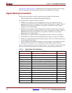
PowerPC 405 Performance
The PowerPC 405 executes instructions at sustained speeds approaching one cycle per
instruction. Table 1-3 lists the typical execution speed (in processor cycles) of the
instruction classes supported by the PowerPC 405.
Instructions that access memory (loads and stores) consider only the “first order” effects of
cache misses. The performance penalty associated with a cache miss involves a number of
second-order effects. This includes PLB contention between the instruction and data