


PowerPC™ 405 Processor Block Reference Guide www.xilinx.com 113
UG018 (v2.0) August 20, 2004 1-800-255-7778
R
C405JTGSHIFTDR (Output)
This output is asserted (logic High) when the PPC405 TAP is in the Shift-DR state. Most
designs do not require this signal and should leave it unconnected.
C405JTGUPDATEDR (Output)
This output is asserted (logic High) when the PPC405 TAP is in the Update-DR state. Most
designs do not require this signal and should leave it unconnected.
C405JTGPGMOUT (Output)
This signal indicates the state of a general purpose program bit in the JTAG debug control
register (JDCR), and is used by some software debuggers. Its function and operation are
determined by the external application. This signal should be left unconnected in most
cases.
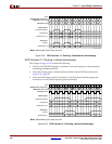
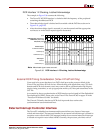
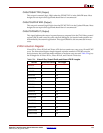
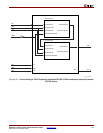
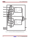
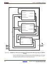
JTAG Instruction Register
Virtex-II Pro, Virtex-II ProX and Virtex-4-FX devices contain zero, one, or two PowerPC405
cores. The Instruction Register length depends upon the number of PPC405 cores the
device features, but it does not matter whether or not those cores are used. Table 2-24 gives
the IR length for all Virtex-II Pro, Virtex-II ProX, and Virtex-4-FX devices.
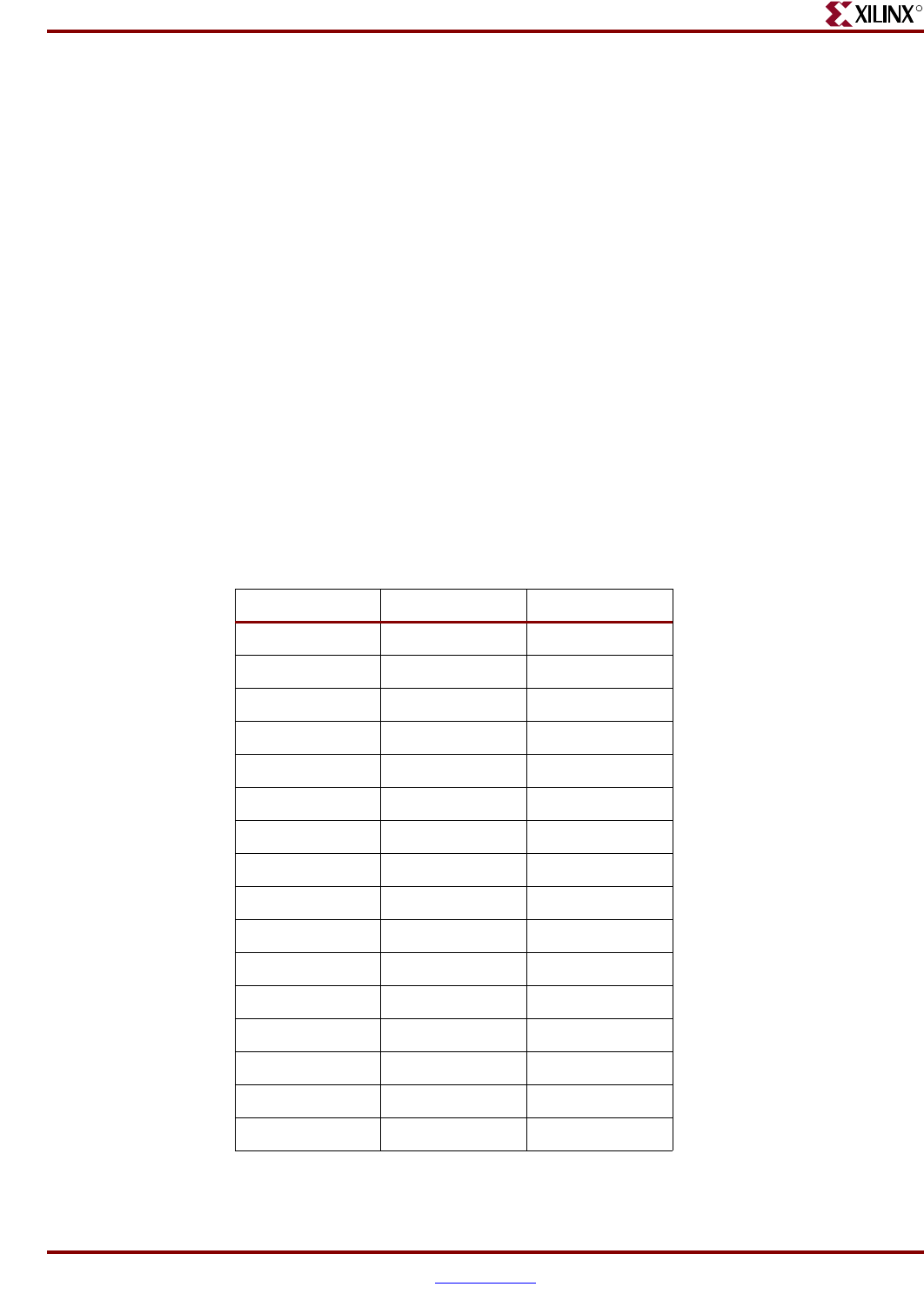
Table 2-24: Virtex-II Pro, Virtex-II ProX, and Virtex-4-FX IR Lengths
Device # PPC405 Cores IR Length
XC2VP2 0 6
XC2VP4 1 10
XC2VP7 1 10
XC2VP20 2 14
XC2VPX20 1 10
XC2VP30 2 14
XC2VP40 2 14
XC2VP50 2 14
XC2VP70 2 14
XC2VPX70 2 14
XC2VP100 2 14
XC4VFX20 1 10
XC4VFX40 1 10
XC4VFX60 1 10
XC4VFX100 2 14
XC4VFX140 2 14