


44 www.xilinx.com PowerPC™ 405 Processor Block Reference Guide
1-800-255-7778 UG018 (v2.0) August 20, 2004
Chapter 2: Input/Output Interfaces
R
JTGC405TRSTNEG signals for at least sixteen clock cycles. FPGA designers cannot modify
the processor block power-on reset mechanism.
The reset logic is not required to support all three types of reset. However, distinguishing
resets by type can make it easier to isolate errors during system debug. For example, a
system could reset the core to recover from an external error that affects software
operation. Following the core reset, a debugger could be used to locate the external error
source that is preserved because neither a chip or system reset occurred.
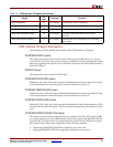
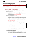
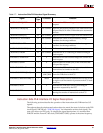
Table 2-5 shows the valid combinations of reset signals and their effect on the DBSR[MRR]
field following reset.
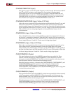
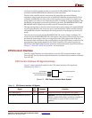
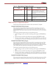
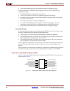
Reset Interface I/O Signal Summary
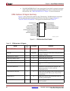
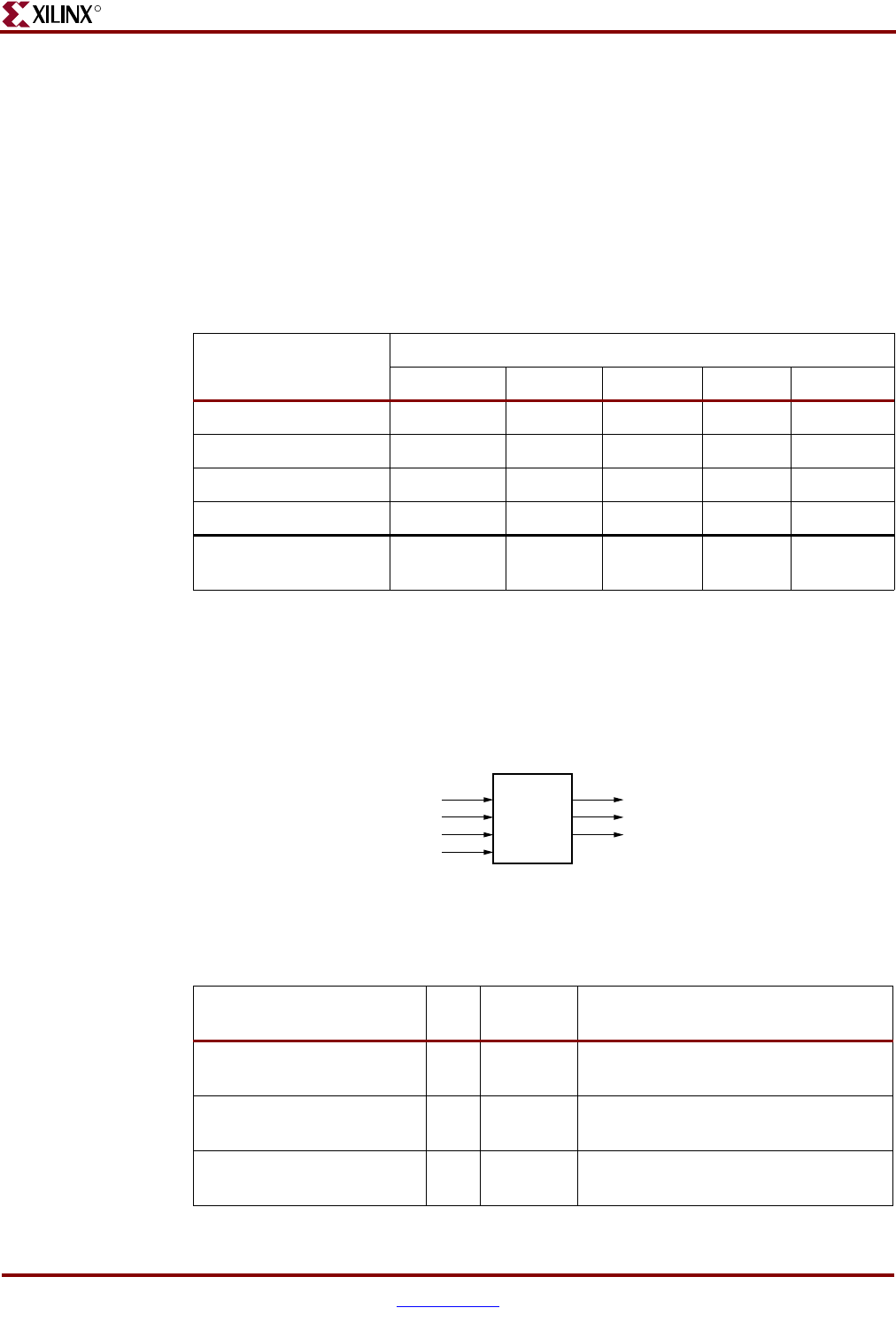
Figure 2-3 shows the block symbol for the reset interface. The signals are summarized in
Table 2-6.
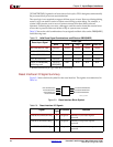
Table 2-5: Valid Reset Signal Combinations and Effect on DBSR(MRR)
Reset Input Signal
Reset Type
None Core Chip System Power-On
a
a. Handled automatically by logic within the processor block.
RSTC405RESETCORE Deassert Assert Assert Assert Assert
RSTC405RESETCHIP Deassert Deassert Assert Assert Assert
RSTC405RESETSYS Deassert Deassert Deassert Assert Assert
JTGC405TRSTNEG Deassert Deassert Deassert Deassert Assert
Value of DBSR[MRR]
following reset
Previous
DBSR[MRR]
0b01 0b10 0b11 0b11
Figure 2-3: Reset Interface Block Symbol
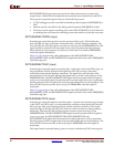
Table 2-6: Reset Interface I/O Signals
Signal
I/O
Type
If Unused Function
C405RSTCORERESETREQ O Required Indicates a core-reset request
occurred.
C405RSTCHIPRESETREQ O Required Indicates a chip-reset request
occurred.
C405RSTSYSRESETREQ O Required Indicates a system-reset request
occurred.
UG018_03_102001
PPC405
RSTC405RESETCORE
RSTC405RESETCHIP
RSTC405RESETSYS
JTGC405TRSTNEG
C405RSTCORERESETREQ
C405RSTCHIPRESETREQ
C405RSTSYSRESETREQ