


176 www.xilinx.com PowerPC™ 405 Processor Block Reference Guide
1-800-255-7778 UG018 (v2.0) August 20, 2004
Chapter 3: PowerPC 405 OCM Controller
R
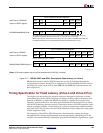
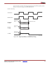
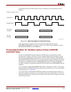
In the figures above, L_addr_n refers to the OCM controller address outputs
DSOCMBRAMRDADDR and Rd_data_n refers to the OCM controller data bus inputs
BRAMDSOCMRDDBUS from the DSBRAMs
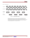
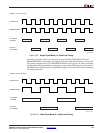
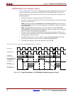
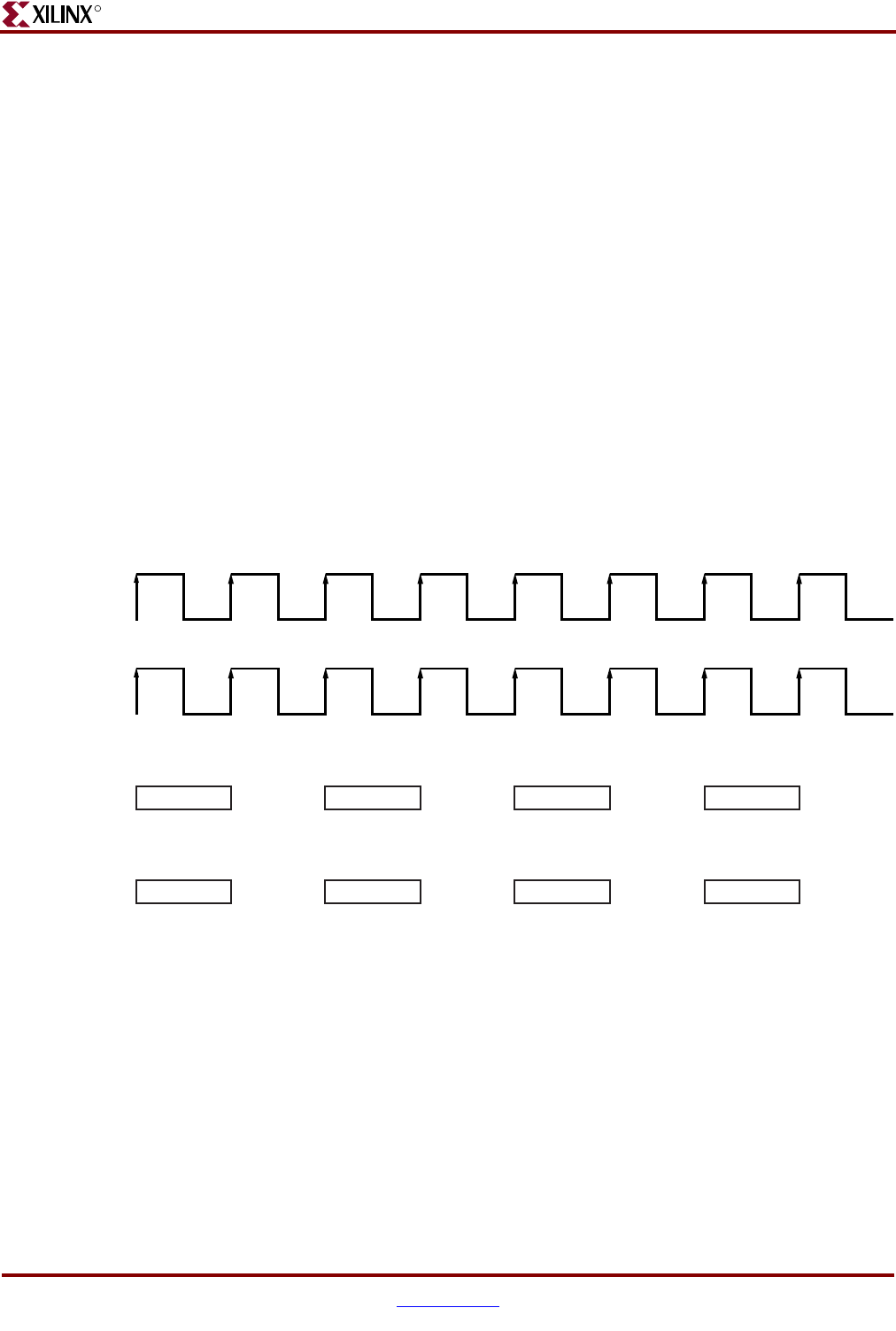
DSOCM Store, Fixed Latency
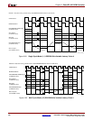
Figure 3-24 and Figure 3-25 below show two back-to-back stores for single-cycle mode and
multi-cycle mode with a CPMC405CLOCK:BRAMDSOCMCLK ratio of 2:1. Note that for
both single cycle and multi-cycle mode, the maximum sustainable store completion is one
store per two BRAMDSOCMCLK periods.
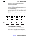
In single-cycle mode the first store requires three processor clock cycles to complete. The
processor core can launch a new address, called back-to-back operation, as soon as the first
address is latched into the OCM controller interface, which is internal to the processor
block. The initial access consists of the following sequence:
1. The CPU launches the store address.
2. The OCM controller translates the CPU order and routes the address, data, and control
signals onto the DSOCM bus.
3. The BRAM stores the data.
In multi-cycle mode, initial wait cycles are inserted until the CPMC405CLOCK and
BRAMDSOCMCLK rising edges are aligned.
After the initial startup latency, one store (32 bits) can be completed every two BRAM clock
cycles, or one store per two BRAMDSOCMCLK clock cycles. In order to estimate the
absolute maximum number of stores per second on the OCM interface, the BRAM clock
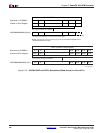
Figure 3-24: Single Cycle Mode (1:1) Data Store Timing
UG018_64_040403
C
PMC405Clock
D
SOCM 1:1 Data Store Timing
B
RAMDSOCMCLK
S
tore Address
(
To BRAM)
W
rite Data
(
To BRAM)
S_addr_1 S_addr_2 S_addr_3 S_addr_4
St_data_1 St_data_2 St_data_3 St_data_4