


PowerPC™ 405 Processor Block Reference Guide www.xilinx.com 85
UG018 (v2.0) August 20, 2004 1-800-255-7778
R
The PLB slave should latch error information in DCRs so that software diagnostic routines
can attempt to report and recover from the error. A bus-error address register (BEAR)
should be implemented for storing the address of the access that caused the error. A bus-
error syndrome register (BESR) should be implemented for storing information about
cause of the error.
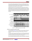
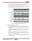
Data-Side PLB Interface Timing Diagrams
The following timing diagrams show typical transfers that can occur on the DSPLB
interface between the DCU and a bus-interface unit (BIU). These timing diagrams
represent the optimal timing relationships supported by the processor block. The BIU can
be implemented using the FPGA processor local bus (PLB) or using customized hardware.
Not all BIU implementations support these optimal timing relationships.
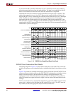
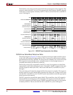
DSPLB Timing Diagram Assumptions
The following assumptions and simplifications were made in producing the optimal
timing relationships shown in the timing diagrams:
x Requests are acknowledged by the BIU in the same cycle they are presented by the
DCU if the BIU is not busy. This represents the earliest cycle a BIU can acknowledge a
request. If the BIU is busy, the request is acknowledged in a later cycle.
x The first read-data acknowledgement for a data read is asserted in the cycle
immediately following the read-request acknowledgement. This represents the
earliest cycle a BIU can begin transferring data to the DCU in response to a read
request. However, the earliest the FPGA PLB begins transferring data is two cycles
after the read request is acknowledged.
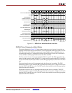
x Subsequent read-data acknowledgements for eight-word line transfers are asserted in
the cycle immediately following the prior read-data acknowledgement. This
represents the fastest rate at which a BIU can transfer data to the DCU (there is no
limit to the number of cycles between two transfers).
x The first write-data acknowledgement for a data write is asserted in the same cycle as
the write-request acknowledgement. This represents the earliest cycle a BIU can begin
accepting data from the DCU in response to a write request.
x Subsequent write-data acknowledgements for eight-word line transfers are asserted
in the cycle immediately following the prior write-data acknowledgement. This
represents the fastest rate at which the DCU can transfer data to the BIU (there is no
limit to the number of cycles between two transfers).
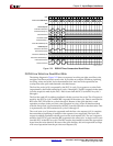
x All eight-word line reads assume the target data (word) is returned first. Subsequent
data in the line is returned sequentially by address, wrapping as necessary to the
lower addresses in the same line.
x The transfer of read data from the fill buffer to the data cache (fill operation) takes
three cycles. This transfer takes place after all data is read into the fill buffer from the
BIU.
x The queuing of data flushed from the data cache (flush operation) takes two cycles.
The PowerPC 405 can queue up to two flush operations.
x The BIU size (bus width) is 64 bits, so PLBC405DCUSSIZE1 is not shown.
x No data-access errors occur, so PLBC405DCUERR is not shown.
x The abort signal, C405PLBDCUABORT is shown only in the last example.
x The storage attribute signals are not shown.