PowerPC™ 405 Processor Block Reference Guide www.xilinx.com 101
UG018 (v2.0) August 20, 2004 1-800-255-7778
R
blocks that are associated with each PowerPC. Thus, this interface is not available to the
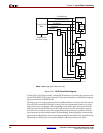
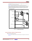
user for connection to the FPGA fabric. Figure 2-29 shows the block symbol for the
dedicated EMAC DCR interface.
For more information on DCR functionality in the EMAC controller, refer to the separate
Virtex-4 EMAC documentation.
In Virtex-4-FX, a DCR access addressing the internal DCR logic will not be visible on the
external DCR bus interface as an access.
External DCR Bus Interface
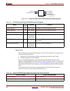
The DCR interface of CoreConnect DCR bus peripherals consists of the following:
x A 10-bit address bus.
x Separate 32-bit input and output data busses.
x Separate read and write control signals.
x A read/write acknowledgement signal.
On Virtex-4-FX parts there is also a clock associated with the interface: CPMDCRCLK (see
the “Clock and Power Management Interface” section of this chapter).
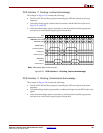
The preferred implementation of the DCR data bus is as a distributed, multiplexed chain.
Each peripheral in the chain has a DCR input-data bus connected to the DCR output-data
bus of the previous peripheral in the chain (the first peripheral is attached to the processor
block). Each peripheral multiplexes this bus with the outputs of its DCRs and passes the
resulting DCR bus as an output to the next peripheral in the chain. The last peripheral in
the chain has its DCR output-data bus attached to the processor block DCR input-data
interface. This implementation enables future DCR expansion without requiring changes
to I/O devices due to additional loading.
There are two options for connecting the acknowledge signals. The acknowledge signals
from the DCRs can be latched and forwarded in the chain with the DCR data bus.
Alternatively, combinatorial logic, such as OR gates, can be used to combine and forward
the acknowledge signal to the processor block.
Figure 2-30 shows an example DCR chain implementation in an FPGA chip. The
acknowledge signal in this example is formed using combinatorial logic (OR gate).
Figure 2-29: Dedicated EMAC DCR Bus Interface Block Symbol
PPC405
EMACDCRACK
EMACDCRDATA
DCREMACCLK
DCREMACENABLER
DCREMACREAD
DCREMACWRITE
DCREMACABUS
DCREMACDBUS
UG018_02_29_042304
Note: This block symbol is provided for completeness. Though not available to the user, the user
will be able to see these signals when modeling the hardware.


