


PowerPC™ 405 Processor Block Reference Guide www.xilinx.com 73
UG018 (v2.0) August 20, 2004 1-800-255-7778
R
Data-Side PLB Interface I/O Signal Descriptions
The following sections describe the operation of the data-side PLB interface I/O signals.
Throughout these descriptions and unless otherwise noted, the term clock refers to the PLB
clock signal, PLBCLK. See “PLBCLK (Input)” for information on this clock signal. The term
cycle refers to a PLB cycle. To simplify the signal descriptions, it is assumed that PLBCLK
and the PowerPC 405 clock (CPMC405CLOCK) operate at the same frequency.
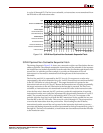
C405PLBDCUREQUEST (Output)
When asserted, this signal indicates the DCU is presenting a data-access request to a PLB
slave device. The PLB slave asserts PLBC405DCUADDRACK to acknowledge the request.
The request can be acknowledged in the same cycle it is presented by the DCU. The request
is deasserted in the cycle after it is acknowledged by the PLB slave. When deasserted, no
unacknowledged data-access request exists.
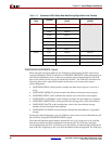
The following output signals contain information for the PLB slave device and are valid
when the request is asserted. The PLB slave must latch these signals by the end of the same
cycle it acknowledges the request:
x C405PLBDCURNW, which specifies whether the data-access request is a read or a
write.
x C405PLBDCUABUS[0:31], which contains the address of the data-access request.
x C405PLBDCUSIZE2, which indicates the transfer size of the data-access request.
x C405PLBDCUCACHEABLE, which indicates whether the data address is cacheable.
x C405PLBDCUWRITETHRU, which specifies the caching policy of the data address.
x C405PLBDCUU0ATTR, which indicates the value of the user-defined storage
attribute for the instruction-fetch address.
x C405PLBDCUGUARDED, which indicates whether the data address is in guarded
storage.
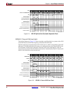
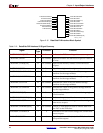
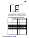
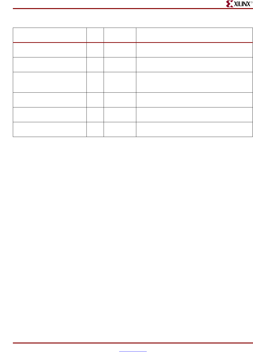
PLBC405DCURDDACK I 0 Indicates the DCU read-data bus contains valid data
for transfer to the DCU.
PLBC405DCURDDBUS[0:63] I 0x0000_0000
_0000_0000
The DCU read-data bus used to transfer data from the
PLB slave to the DCU.
PLBC405DCURDWDADDR[1:3] I 0b000 Indicates which word or doubleword of an eight-
word line transfer is present on the DCU read-data
bus.
PLBC405DCUWRDACK I 0 Indicates the data on the DCU write-data bus is being
accepted by the PLB slave.
PLBC405DCUBUSY I 0 Indicates the PLB slave is busy performing an
operation requested by the DCU.
PLBC405DCUERR I 0 Indicates an error was detected by the PLB slave
during the transfer of data to or from the DCU.
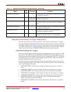
Table 2-12: Data-Side PLB Interface I/O Signal Summary (Continued)
Signal
I/O
Type
If Unused Function