


170 www.xilinx.com PowerPC™ 405 Processor Block Reference Guide
1-800-255-7778 UG018 (v2.0) August 20, 2004
Chapter 3: PowerPC 405 OCM Controller
R
routing delays, signal loading, BRAM memory access time, clock to output times, and
setup and hold times of the BRAM and processor blocks. Users may need to go through
multiple iterations of evaluating OCM BRAM size versus OCM clock frequency in order to
achieve the optimum performance.
The clock ratio between the BRAM clock and the PPC405 is auto-detected in Virtex-4 when
control register bit 3 is set to 1 (DSCNTL and ISCNTL). For Virtex-II Pro, bits 5 to 7 are used
to set the clock ratio. Refer to the “Programmer's Model” section for further details.
Single-Cycle Mode
In single-cycle mode, the CPU core, OCM controllers, and BRAMs all run at the same clock
speed. Typically, the processor runs at a slower speed than its maximum specified
operating frequency, in order to match the speed of the OCM to BRAM interface. The
processor frequency must always be reduced when operating in single cycle mode, even
when using the smallest supported configuration of DSBRAMs or ISBRAMs.
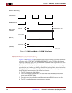
Multi-Cycle Mode
Multi-cycle mode permits the processor to run at its maximum specified operating
frequency. Based upon application specific timing analysis, the clock frequency for the
OCM controllers and attached BRAMs is reduced to an integer multiple of the processor
clock. Wait states are inserted between each instruction fetch, data load, or data store
transaction, internal to the processor block. The transactions start and end on rising clock
edges of the processor clock and the OCM clock. The Digital Clock Manager (DCM) should
be used to generate the clocks for the CPU core, OCM controllers, DSBRAMs, and
ISBRAMs. Additionally, an identical clock must be applied to an OCM controller (DSOCM
or ISOCM) and its corresponding BRAMs for any mode described above. Each controller
(DSOCM or ISOCM) can be clocked at a frequency independent of the other.
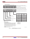
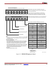
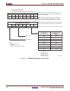
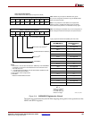
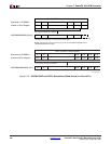
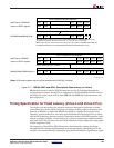
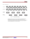
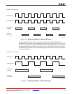
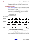
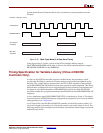
ISOCM Instruction Fetching
The figures below show two back to back instruction fetches for single-cycle mode
(Figure 3-18) and multi-cycle mode with CPMC405CLOCK:BRAMISOCMCLK ratio of 2:1
(Figure 3-19). Note that for both single-cycle and multi-cycle mode, the maximum
sustainable instruction fetch rate is one instruction per BRAMISOCMCLK period. For
designs that utilize other integer clock ratios, note that the rising edge of the
BRAMISOCMCLK defines the bus cycle, as the timing diagram illustrates.
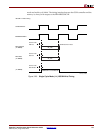
In single-cycle mode the very first instruction fetch requires four processor clock cycles to
complete. The processor core can launch a new address, called “back-to-back operation,”
as soon as the first address is latched into the OCM controller interface, which is internal to
the processor block. The initial access consists of the following sequences:
1. The CPU launches the instruction fetch address.
2. The OCM controller translates the CPU order and routes the address and control
signals onto the ISOCM bus.
3. One wait state is introduced to permit the synchronous BRAM to access the data.
4. The CPU stores the data.