


102 www.xilinx.com PowerPC™ 405 Processor Block Reference Guide
1-800-255-7778 UG018 (v2.0) August 20, 2004
Chapter 2: Input/Output Interfaces
R
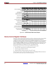
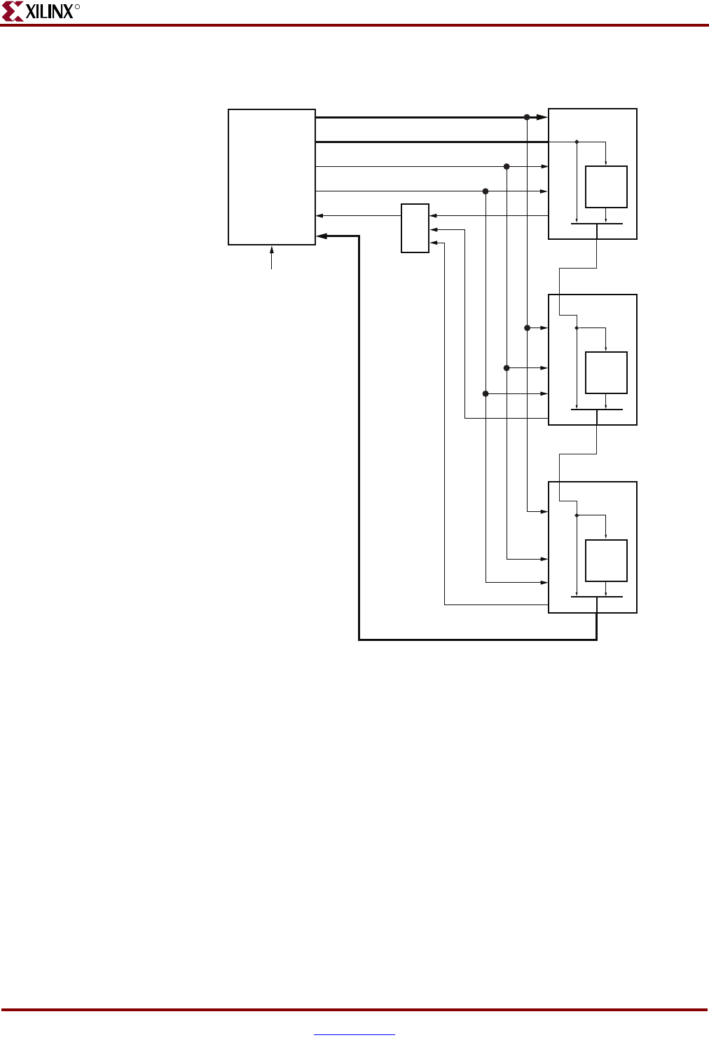
In Virtex-II Pro/ProX the PowerPC external DCR interface is clocked by the processor core
clock (CPMC405CLOCK), but in Virtex-4-FX the external interface is clocked by an input to
the processor block (CPMDCRCLK).
DCR slaves can use clock frequencies that are different (faster or slower) from the one the
PowerPC 405 external DCR interface is using. The only requirement is that every rising
edge of the slower clock align with a rising edge of the faster clock. This means that the
clocks for the external DCR slaves and the clock for the PowerPC 405 interface must be
derived from a common source. The reason different frequencies are possible is that the
access protocol of the bus implements full handshaking, meaning that the Acknowledge
signal sent on a Read/Write access is only deasserted after the Read/Write signal has been
deasserted. If a DCR access is not acknowledged within 64 processor core cycles
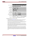
Figure 2-30: DCR Chain Block Diagram
DCRs
DCR Slave 1
DCRs
DCR Slave 2
DCRs
DCR Slave 3
OR
PowerPC 405
Block
CPMDCRCLK
(for Virtex-4 only)
DCRACK
DCRDBUSIN[0:31]
DCRREAD
DCRWRITE
DCRDBUSOUT[0:31]
DCRABUS[0:9]
UG018_52_042304
Note: Abbreviated signal names are used.