


1-20
Introduction
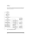
Status Reporting
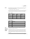
Acquisition Event
Register (AER)
Bit 0 (COMP) of the Acquisition Event Register is set when the acquisition limits complete.
The Acquisition completion criteria are set by the ACQuire:RUNtil command. Refer to
“RUNTil” on page 6-4. The Acquisition Event Register is read and cleared with the ALER?
query. Refer to “ALER?” on page 4-3.
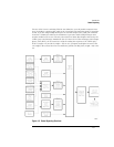
Clock Recovery
Event Register
(CRER)
This register hosts the UNLK bit (bit 0), LOCK bit (bit 1), NSPR1 bit (bit 2), SPR1 bit (bit 3),
NSPR2 bit (bit 4) and SPR2 (bit 5). Bit 0 (UNLK) of the Clock Recovery Event Register is set
when an 83491/2/3/4/5/6A clock recovery module becomes unlocked or trigger loss has
occurred. Bit 1 (LOCK) of the Clock Recovery Event Register is set when a clock recovery
module becomes locked or a trigger capture has occurred. If an 83496A module is locked,
sending the CRECovery:RELock command does not set UNLK bit (bit 0) or LOCK bit (bit 1).
To determine if the RELock command has completed, use the CRECovery:LOCKed? query.
Refer to “RELock” on page 9-9.
Bits 2 through 5 provide information on optical signals and so are not effected by 83495A
modules. Bit 2 (NSPR1) of the Clock Recovery Event Register is set when an clock recovery
module transitions to no longer detecting an optical signal on receiver one. Bit 3 (SPR1) of
the Clock Recovery Event Register is set when an clock recovery module transitions to
detecting an optical signal on receiver one. Bit 4 (NSPR2) of the Clock Recovery Event Regis-
ter is set when an clock recovery module transitions to no longer detecting an optical signal
on receiver two. Bit 5 (SPR2) of the Clock Recovery Event Register is set when an clock
recovery module transitions to detecting an optical signal on receiver two. The Clock Recov-
ery Event Register is read and cleared with the CRER? query. Refer to “CRER?” on page 4-6.
When either of the UNLK, LOCK, NSPR1, SPR1, NSPR2 or SPR2 bits are set, they in turn set
CLCK bit (bit 7) of the Operation Status Register. Results from the Clock Recovery Event
Register can be masked by using the CREE command to set the Clock Recovery Event
Enable Register. Refer to Refer to “CREE” on page 4-5 for enable and mask value definitions.
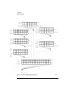
Limit Test Event
Register (LTER)
Bit 0 (COMP) of the Limit Test Event Register is set when the Limit Test completes. The
Limit Test completion criteria are set by the LTESt:RUN command. Refer to “RUNTil” on
page 15-4. Bit 1 (FAIL) of the Limit Test Event Register is set when the Limit Test fails. Fail-
ure criteria for the Limit Test are defined by the LTESt:FAIL command. Refer to “FAIL” on
page 15-2. The Limit Test Event Register is read and cleared with the LTER? query. Refer to
“LTER?” on page 4-9. When either the COMP or FAIL bits are set, they in turn set the LTEST
bit (bit 8) of the Operation Status Register. You can mask the COMP and FAIL bits, thus pre-
venting them from setting the LTEST bit, by defining a mask using the LTEE command. Refer
to “LTEE” on page 4-9. When the COMP bit is set, it in turn sets the ACQ bit (bit 9) of the
Operation Status Register. Results from the Acquisition Register can be masked by using the
AEEN command to set the Acquisition Event Enable Register to the value 0. You enable the
COMP bit by setting the mask value to 1.
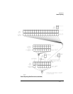
Jitter Event
Register (JIT)
Bit 0 (EFAIL) of the Jitter Event Register is set when characterizing edges in Jitter Mode
fails. Bit 1 (JLOSS) of the register is set when pattern synchronization is lost in Jitter Mode.
Bit 2 (AREQD) of the register is set when a parameter change in Jitter Mode has made
autoscale necessary. Bit 12 of the Operation Status Register (JIT) indicates that one of the