


PXA250 and PXA210 Applications Processors Design Guide A-3
SA-1110/Applications Processor Migration
The power fault (VDD_FAULT) and battery fault (BATT_FAULT) pins that drive the SA-1110
sleep mode are negated with respect to the PXA250 applications processor. You must invert these
signals or change the design to make sure that these signals are negated with respect to the SA-
1110 design.
The PXA250 applications processor treats variable latency IO differently than the SA-1110. The
difference occurs only when a static chip select is configured to support variable latency IO, i.e. the
bus cycle is to be extended by a value on the RDY pin. In this configuration, the SDRAM refresh
cycle retains the use of the nWE pin to allow the memory bus to be held for an indeterminate time.
During any variable latency IO cycle, the PCMCIA pin nPWE is used to write to an external device
instead of the nWE pin.
Note: Holding the bus for extended periods is not recommended because it interferes with the LCD DMA
and prevents an LCD panel refresh.
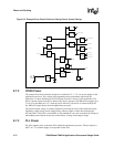
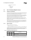
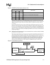
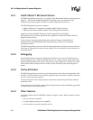
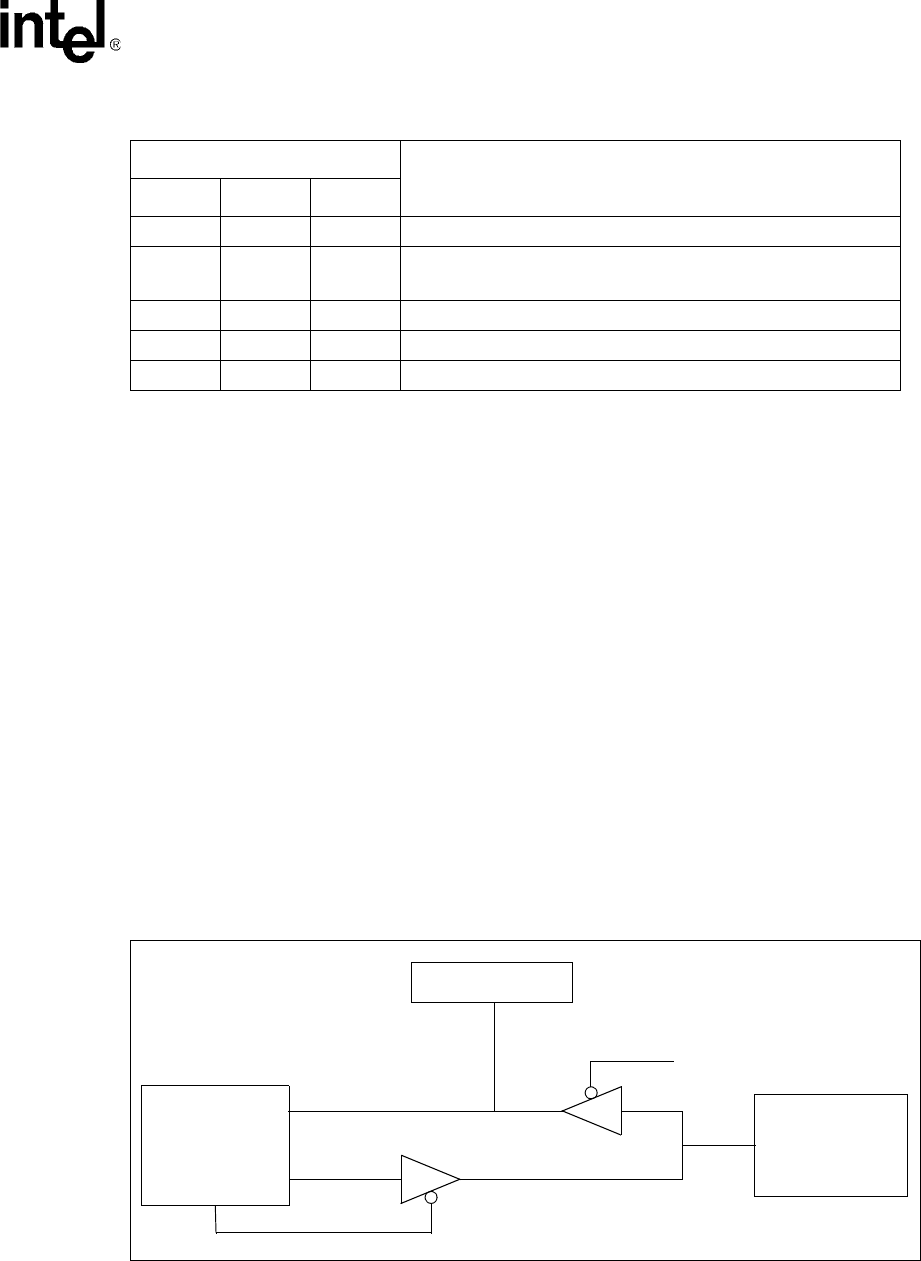
This change in write enables only causes an issue if an external companion bus master device has a
single write enable pin and requires variable latency IO to be accessed. As shown in Figure A-1,
the write enable to the companion master has to be gated to differentiate between a case where the
PXA250 applications processor uses the WE to write to the companion and a case where the
companion uses the WE to write into SDRAM memory. Gating the WE pin with the Bus Grant
signal (as shown) segregates the two different memory bus cycle types. If the companion bus
master has both a WE input pin and a WE output pin to SDRAM, this logic is unnecessary.
0 1 1 Synchronous 16-bit Flash
100
(1) Synchronous 32-bit Mask ROM (64 Mbit)
(2) Synchronous 16-bit Mask ROM = 32bits (32 Mbit)
1 0 1 (1) Synchronous 16-bit Mask ROM (64 Mbit)
1 1 0 (2) Synchronous 16-bit Mask ROM = 32bits (64 Mbit)
1 1 1 (1) Synchronous 16-bit Mask ROM (32 Mbit)
Table A-1. PXA250 Boot Select Options (Sheet 2 of 2)
Boot Select Pins
Boot Location
210
Figure A-1. Write Enable Control Pins
SDRAM
PXA250
SA-1110
Companion
Device
nWE
MBGNT
~MBGNT
WE#
nPWE