


1-8 PXA250 and PXA210 Applications Processors Design Guide
Introduction
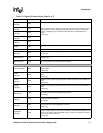
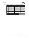
SDA ICOCZ
I2C Data signal (bidirectional).
Bidirectional signal. When it is driving, it functions as an open collector device and
requires a pull up resistor. As an input, it expects standard CMOS levels.
PWM Pins
PWM[1:0]/
GPIO[17,16]
ICOCZ
Pulse Width Modulation channels 0 and 1 (outputs)
See Note [2]
Dedicated GPIO Pins
GPIO[1:0] ICOCZ
General Purpose I/O: These two pins are contained in both the PXA250
and PXA210
applications processors. They are preconfigured at a hard reset (nRESET) as wakeup
sources for both rising and falling edge detects.
These GPIOs do not have alternate functions and are intended to be used as the main
external sleep wakeup stimulus.
GPIO[14:2]) ICOCZ
General Purpose I/O
See Note [1]
See Note [2]
GPIO[22:21] ICOCZ
General Purpose I/O
Additional general purpose I/O pins.
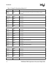
Crystal Pins
PXTAL IA Input connection for 3.6864 Mhz crystal
PEXTAL OA Output connection for 3.6864 Mhz crystal
TXTAL IA Input connection for 32.768 khz crystal
TEXTAL OA Output connection for 32.768 khz crystal
48MHz/GP[7] ICOCZ 48 MHz clock. (output) Peripheral clock output derived from the PLL.
RTCCLK/GP[10] ICOCZ Real time clock. (output) HZ output derived from the 32kHz or 3.6864MHz output.
3.6MHz/GP[11] ICOCZ 3.6864 MHz clock. (output) Output from 3.6864 MHz oscillator.
32kHz/GP[12] ICOCZ 32 kHz clock. (output) Output from the 32 kHz oscillator.
Miscellaneous Pins
BOOT_SEL
[2:0]
IC
Boot programming select pins. These pins are sampled to indicate the type of boot
device present per the following table;
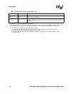
BOOT_SEL[2:0] Description
000Asynchronous 32-bit ROM
001Asynchronous 16-bit ROM
100One 32-bit SMROM
101One 16 bit SMROM
110Two 16 bit SMROMs (32 bit bus)
111Reserved
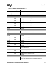
PWR_EN OCZ
Power Enable. Active high Output.
PWR_EN enables the external power supply. Negating it signals the power supply
that the system is going into sleep mode and that the VDD power supply should be
removed.
nBATT_FAULT IC
Battery Fault. Active low input.
The assertion of nBATT_FAULT causes the applications processor
to enter Sleep
Mode.The applications processor
will not recognize a wakeup event while this signal
is asserted. Use nBATT_FAULT signal to flag a critical power failure, such as the main
battery being removed. Minimum assertion time for nBATT_FAULT is 1ms.
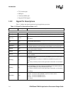
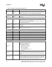
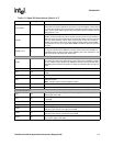
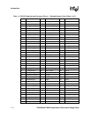
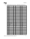
Table 1-3. Signal Pin Descriptions (Sheet 5 of 7)
Name Type Description