


PXA250 and PXA210 Applications Processors Design Guide 2-1
System Memory Interface 2
This section is the design guidelines for the system memory interface.
2.1 Overview
The external memory bus interface for the applications processor supports:
• 100 MHz SDRAM at 3.3 V
• 100 MHz SDRAM at 2.5 V
• Synchronous and asynchronous Burst mode and Page mode Flash
• Synchronous Mask ROM (SMROM)
• Page Mode ROM
• SRAM
• SRAM-like Variable Latency I/O (VLIO)
• PCMCIA expansion memory
• Compact Flash
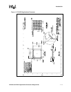
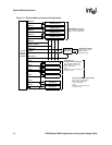
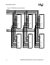
Use the memory interface configuration registers to program the memory types. Refer to
Figure 1-1, “Applications Processor Block Diagram” on page 1-2 for the block diagram of the
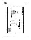
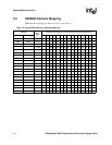
Memory Controller configuration. Refer to Figure 2-1, “Memory Address Map” on page 2-3 for
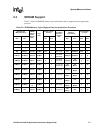
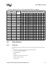
the applications processor memory map. Refer to Table 2-3, “Normal Mode Memory Address
Mapping” on page 2-6 for alternate mode address mapping.